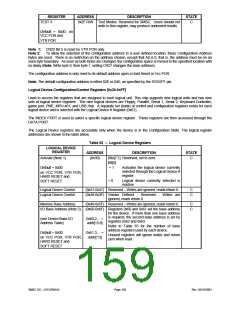
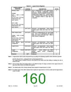
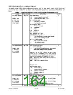
Table 64 – Logical Device Registers
ADDRESS DESCRIPTION
(0x70,0x72) 0x70 is implemented for each logical device.
Refer to Interrupt Configuration Register
description. Only the keyboard controller uses
Interrupt Select register 0x72. Unused register
(0x72) will ignore writes and return zero when
read. Interrupts default to edge high (ISA
compatible).
LOGICAL DEVICE
REGISTER
Interrupt Select
STATE
C
Defaults :
0x70 = 0x00 or 0x06
(Note 3)
on VCC POR, VTR POR,
HARD RESET and
SOFT RESET
0x72 = 0x00,
on VCC POR, VTR POR,
HARD RESET and
SOFT RESET
(0x71,0x73) Reserved - not implemented. These register
locations ignore writes and return zero when
read.
(0x74,0x75) Only 0x74 is implemented for FDC and Parallel
port. 0x75 is not implemented and ignores
writes and returns zero when read. Refer to
DMA Channel Configuration.
DMA Channel Select
C
Default = 0x02 or 0x04
(Note 4)
on VCC POR, VTR POR,
HARD RESET and
SOFT RESET
32-Bit Memory Space (0x76-0xA8) Reserved - not implemented. These register
Configuration
locations ignore writes and return zero when
read.
Logical Device
(0xA9-0xDF) Reserved - not implemented. These register
locations ignore writes and return zero when
read.
C
C
C
Logical
Device (0xE0-0xFE) Reserved
–
Vendor Defined (see SMSC
Configuration
defined
Logical Device Configuration
Registers).
Reserved
0xFF
Reserved
Note 1: A logical device will be active and powered up according to the following equation unless otherwise specified:
DEVICE ON (ACTIVE) = (Activate Bit SET or Pwr/Control Bit SET).
The Logical device's Activate Bit and its Pwr/Control Bit are linked such that setting or clearing one sets or
clears the other.
Note 2: If the I/O Base Addr of the logical device is not within the Base I/O range as shown in the Logical Device I/O
map, then read or write is not valid and is ignored.
Note 3: The default value of the Primary Interrupt Select register for logical device 0 is 0x06.
Note 4: The default value of the DMA Channel Select register for logical device 0 (FDD) is 0x02 and for logical device
3 and 5 is 0x04.
SMSC DS – LPC47M14X
Page 160
Rev. 03/19/2001

 SMSC [ SMSC CORPORATION ]