Note 9: If this pin is used for Ring Indicator wakeup, either the nRI2 event can be enabled via bit 1 in the PME_EN1
register or the GP50 PME event can be enabled via bit 0 in the PME_EN5 register.
Note 10: In order to use the P12, P16 and P17 functions, the corresponding GPIO must be programmed for output,
non-invert, and push-pull output type.
The P17 function should not be selected on GP20 and GP 62 simultaneously. If P17 is selected on GP20 and GP62,
simultaneously, then P17 on GP62 will function and P17 on GP20 will not.
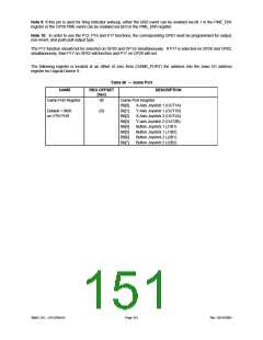
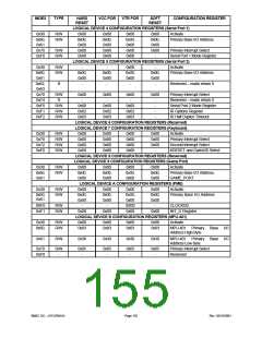
The following register is located at an offset of zero from (GAME_PORT) the address into the base I/O address
register for Logical Device 9.
Table 60 – Game Port
NAME
REG OFFSET
(hex)
DESCRIPTION
Game Port Register
00
Game Port Register
Bit[0]
Bit[1]
Bit[2]
Bit[3]
Bit[4]
Bit[5]
Bit[6]
Bit[7]
X-Axis Joystick 1 (OUT1A)
Y-Axis Joystick 1 (OUT1B)
X-Axis Joystick 2 (OUT2A)
Y-axis Joystick 2 (OUT2B)
Button Joystick 1 (J1B1)
Button Joystick 1 (J1B2)
Button Joystick 2 (J2B1)
Button Joystick 2 (J2B2)
Default = 0x00
on VTR POR
(R)
SMSC DS – LPC47M14X
Page 151
Rev. 03/19/2001

 SMSC [ SMSC CORPORATION ]