14 LPC47M14X REVISIONS
DATE
PAGE(S)
SECTION/FIGURE/ENTRY
CORRECTION
See italicized text
See italicized text
REVISED
03/19/01
03/19/01
03/19/01
1
3
10
Features
General Description
DESCRIPTION OF PIN FUNCTIONS
Changes to Note 4 (see
italicized text)
21
22
Field Definitions
See italicized text
03/19/01
03/19/01
I/O Read and Write Cycles, DMA Read and See the “Low Pin Count
Write Cycles, CLOCKRUN Protocol, LPCPD (LPC) Interface
Protocol, SYNC Protocol
Specification” Revision
1.0 (See italicized text)
23
34
I/O Transfers
Bit 5 Non-DMA
See italicized text
03/19/01
03/19/01
Reserved, read ‘0’.
This part does not
support non-DMA
mode.
40
41
Non-DMA Mode - Transfers from the FIFO to This part does not
03/19/01
03/19/01
the Host, Non-DMA Mode - Transfers from the support non-DMA
Host to the FIFO
mode.
Table 17
–
Description of Command Non-DMA Mode Flag -
Write ‘0’. This part does
not support non-DMA
Symbols
mode.
94
POWER MANAGEMENT
Note added (see
03/19/01
italicized text)
113
119
Note 5 under table
(see italicized text)
03/19/01
03/19/01
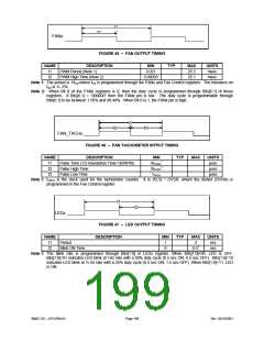
Fan Tachometer Inputs, second paragraph The divisor for each fan
under fan count equation
is programmable via
the Fan Control
Register, which is
located in the Runtime
Register block at offset
0xFA.
125
127
156
Table 58
Summary
–
Runtime Register Block Changes to Note 5 (see
03/19/01
03/19/01
03/19/01
italicized text)
Table 59 – PME, SMI, GPIO, FAN Register Changes to Note 6 (see
Description
italicized text)
Table 62 – Chip Level Registers
0x22 R/W Address - 0:
Power Off or Disabled
1: Power On or
Enabled
0x23 R/W Address -
(see Note in the “FDC
Power Management”
section.)
168
172
Table 72 – KYBD, Logical Device 7 [Logical KRST_GA20 - Bits[6:5]
03/19/01
03/19/01
Device Number = 0x07]
DC Electrical Characteristics
reset on VTR POR only
Values added to:
V
CC Supply Current
Active, VTR Supply
Current Active and VREF
Supply Current Active
200
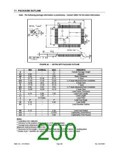
PACKAGE OUTLINE
Note added (see
italicized text)
03/19/01
SMSC DS – LPC47M14X
Page 205
Rev. 03/19/2001

 SMSC [ SMSC CORPORATION ]