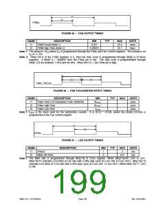
t1
t2
FANx
FIGURE 45 – FAN OUTPUT TIMING
NAME
t1
t2
DESCRIPTION
PWM Period (Note 1)
PWM High Time (Note 2)
MIN
0.021
0.00033
TYP
MAX
25.5
25.1
UNITS
msec
msec
Note 1: The period is 1/fout,where fout is programmed through the FANx and Fan Control registers. The tolerance on
fout is +/- 2%.
Note 2: When Bit 0 of the FANx registers is 0, then the duty cycle is programmed through Bits[6:1] of these
registers. If Bits[6:1] = “000000” then the FANx pin is low. The duty cycle is programmable through
Bits[6:1] to be between 1.56% and 98.44%. When Bit 0 is 1, the FANx pin is high.
t1
t2
t3
FAN_TACHx
FIGURE 46 – FAN TACHOMETER INTPUT TIMING
NAME
DESCRIPTION
Pulse Time (1/2 Revolution Time=30/RPM)
Pulse High Time
MIN
4tTACH
3tTACH
tTACH
TYP
MAX
UNITS
µsec
µsec
1
1
t1
t2
t3
Pulse Low Time
µsec
Note 1: tTACH is the clock used for the tachometer counter. It is 30.52 * DVSR, where the divisor (DVSR) is
programmed in the Fan Control register.
t1
t2
LEDx
FIGURE 47 – LED OUTPUT TIMING
NAME
t1
t2
DESCRIPTION
MIN
1
0
TYP
MAX
2
UNITS
sec
sec
Period
Blink ON Time
0.51
Note 1: The blink rate is programmed through Bits[1:0] in LEDx register. When Bits[1:0]=00, LED is OFF.
Bits[1:0]=01 indicates LED blink at 1Hz rate with a 50% duty cycle (0.5 sec ON, 0.5 sec OFF). Bits[1:0]=10
indicates LED blink at ½ Hz rate with a 25% duty cycle (0.5 sec ON, 1.5 sec OFF). When Bits[1:0]=11, LED
is ON.
SMSC DS – LPC47M14X
Page 199
Rev. 03/19/2001

 SMSC [ SMSC CORPORATION ]