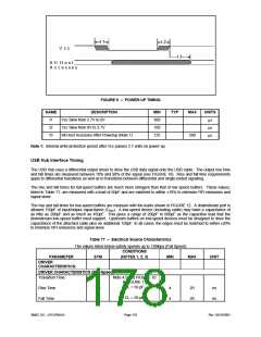
t 1
t 2
V c c
t 3
A ll H o s t
A c c e s s e s
FIGURE 9 – POWER-UP TIMING
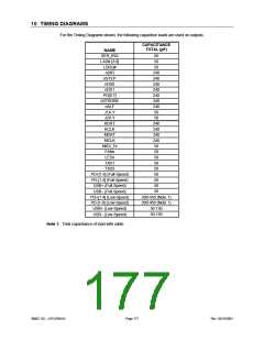
NAME
DESCRIPTION
MIN
300
100
125
TYP
MAX
UNITS
µs
t1
t2
t3
Vcc Slew from 2.7V to 0V
Vcc Slew from 0V to 2.7V
µs
All Host Accesses After Powerup (Note 1)
500
µs
Note 1: Internal write-protection period after Vcc passes 2.7 volts on power-up
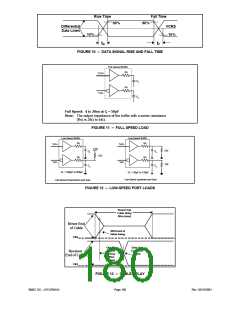
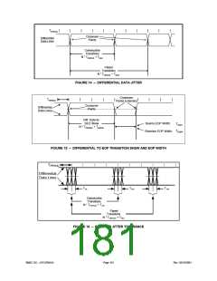
USB Hub Interface Timing
The USB Hub uses a differential output driver to drive the USB data signal onto the USB cable. The output rise time
and fall times are measured between 10% and 90% of the signal (see FIGURE 10). Rise and fall time requirements
apply to differential transitions as well as to transitions between differential and single-ended signaling.
The rise and fall times for full-speed buffers are much more stringent than that of low speed buffers. These values,
listed in Table 77, are measured with a load of 50pF and are matched to within ±10% to minimize RFI emissions and
signal skew.
The rise and fall times for low-speed buffers are measure with the loads shown in FIGURE 12. A downstream port is
allowed 150pF of input/output capacitance (CIND). A low-speed device (including cable) may have a capacitance of
as little as 200pF and as much as 450pF. This gives a range of 200pF to 600pF as the capacitive load that the
downstream low-speed buffer must support. Upstream buffers on low-speed devices must be designed to drive the
capacitance of the attached cable plus an additional 150pF. In all cases, the edges must be matched to within ±20%
to minimize RFI emissions and signal skew.
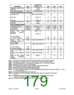
Table 77 – Electrical Source Characteristics
The values listed below satisfy speeds up to 12Mbps (Full Speed)
CONDITIONS
PARAMETER
DRIVER
CHARACTERISTICS:
SYM
(NOTES 1, 2, 3)
MIN
MAX
UNIT
DRIVER CHARACTERISTICS (Full-Speed)
Transition Time:
Note 4,5 and FIGURE 10
& FIGURE 11
CL = 50 pF
CL = 50 pF
Rise Time
Fall Time
TR
TF
4
4
20
20
ns
ns
SMSC DS – LPC47M14X
Page 178
Rev. 03/19/2001

 SMSC [ SMSC CORPORATION ]