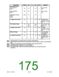
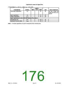
CONDITIONS
(NOTES 1, 2, 3)
(TR/TF)
PARAMETER
SYM
TRFM
MIN
90
MAX
111.11
UNIT
%
Differential Rise/Fall Time
Matching
Note 9
Drive Output Impedance
ZDRV
Steady State Drive
28
44
Ω
DRIVER CHARACTERISTICS (Low-Speed)
Transition Time:
Note 4,5 and FIGURE 10
Rise Time
TR
FIGURE 12
75
300
ns
Fall Time
TF
TRFM
FIGURE 12
(TR/TF)
75
80
300
125
ns
%
Differential Rise/Fall Time
Matching
Note 9
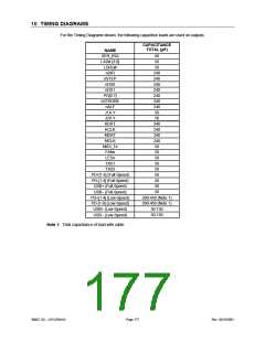
DATA TRANSFER TIMINGS
Full Speed Data Rate
Frame Interval
11.9700
0.9995
80
12.0300
1.0005
86
TDRATE
TFRAME
TPERIOD
Notes 8, 10, & 12
Note 8
Mbs
ms
ns
Clock Period
Note 10
Source
Jitter
Total
Note 6, 7, & 9
(including
tolerance):
frequency
FIGURE 14
To next Transition
TDJ1
TDJ2
TDEOP
-3.5
-4.0
-2
3.5
4.0
5
ns
ns
ns
For Paired Transitions
Source
Jitter
for
Note 7 and FIGURE 15
Note 7 and FIGURE 16
Differential Transition to
SEO Transition
Receiver Jitter:
To next Transition
TJR1
TJR2
TEOPT
-18.5
-9
160
18.5
9.0
175
ns
ns
ns
For Paired Transitions
Source SEO interval of
Note 7 and FIGURE 15
Note 7 and FIGURE 15
Note 11
EOP
Receiver SEO interval of
EOP
TEOPR
TFST
82
ns
ns
Width of SEO interval
14
during
differential
transition
Note 1: All voltages are measured from the local ground potential, unless otherwise specified.
Note 2: All timing use a capacitive load (CL) to ground of 50pF, unless otherwise specified.
Note 3: Full speed timings have a 1.5KΩ pull-up to a voltage of 3.0V - 3.6V on the D+ data line.
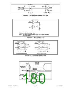
Note 4: Measured from 10% to 90% of the data signals.
Note 5: The rising and falling edges should be smoothly transitioning (monotonic).
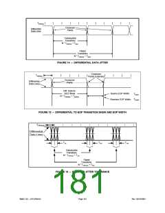
Note 6: Timing differences between the differential data signals.
Note 7: Measured at crossover point of differential data signals.
Note 8: For a more detailed description of the Data Signaling Rate and the Frame Interval see sections 7.1.11 and
7.1.12 in the USB Spec 1.1.
Note 9: Excluding the first transition from the idle state.
Note 10: The accuracy of the host controller’s data rate must be known and controlled to better than
±0.05%
Note 11: During differential signal transitions both PD+ and PD- may temporarily be less that
VIH(min). This period can be up to 14ns.
Note 12: The data-rate tolerance for host, hub, and full-speed functions is ±0.25%
SMSC DS – LPC47M14X
Page 179
Rev. 03/19/2001

 SMSC [ SMSC CORPORATION ]