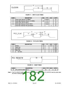
t1
CLOCKI
t2
t2
FIGURE 17 – INPUT CLOCK TIMING
DESCRIPTION MIN
20
NAME
TYP
69.84
35
31.25
16.53
MAX
UNITS
ns
ns
µs
µs
t1
t2
t1
t2
Clock Cycle Time for 14.318MHZ
Clock High Time/Low Time for 14.318MHz
Clock Cycle Time for 32KHZ
Clock High Time/Low Time for 32KHz
Clock Rise Time/Fall Time (not shown)
5
ns
t1
t4
t2
t5
t3
P C I_C LK
FIGURE 18 – PCI CLOCK TIMING
NAME
DESCRIPTION
MIN
30
12
TYP
MAX
33.3
UNITS
nsec
nsec
nsec
nsec
nsec
t1
t2
t3
t4
Period
High Time
Low Time
Rise Time
12
3
3
t5 ꢀ
Fall Time
t4
PCI RESET#
FIGURE 19 – RESET TIMING
NAME
t4
DESCRIPTION
PCI_RESET# width (Note 1)
MIN
TYP MAX
UNITS
µs
Note 1: The PCI_RESET# width is dependent upon the processor clock. The PCI_RESET# must be active while
the clock is running and stable.
SMSC DS – LPC47M14X
Page 182
Rev. 03/19/2001

 SMSC [ SMSC CORPORATION ]