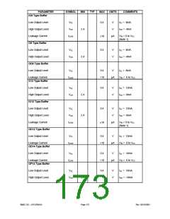
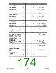
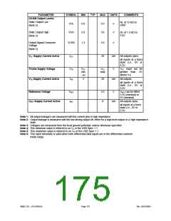
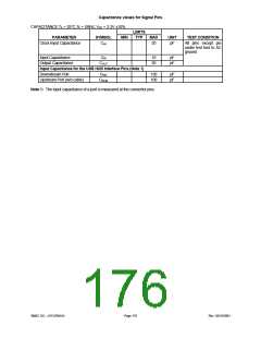
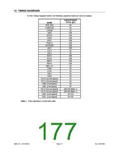
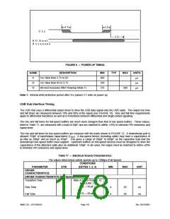
PARAMETER
SYMBOL
MIN
TYP
MAX
UNITS
COMMENTS
IOP14 Type Buffer
Low Output Level
High Output Level
Leakage Current
IOD16 Type Buffer
Low Output Level
Leakage Current
O24 Type Buffer
Low Output Level
High Output Level
VOL
VOH
ILEAK
0.4
V
V
IOL = 14mA
IOH = -14mA
2.4
µA
VIN = 0 to VCC
(Note 1)
±10
VOL
0.4
V
IOL = 16mA
ILEAK
µA
VIN = 0 to VCC
(Note 1)
±10
VOL
0.4
V
IOL = 24 mA @ VCC
VOH
IIL
2.4
V
µA
IOH = -12 mA @ VCC
VCC = 0V
VIN = 5.5V Max
Backdrive
± 10
Protect/ChiProtect
(All signal pins excluding
LAD[3:0], LDRQ#, LPCPD#,
LFRAME#,
USB+,
USB-,
PD+[1:4], PD-[1:4])
5V Tolerant Pins
IIL
± 10
± 10
µA
µA
VCC = 3.3V
(All signal pins excluding
VIN = 5.5V Max
LAD[3:0], LDRQ#, LPCPD#,
LFRAME#,
USB+,
USB-,
PD+[1:4], PD-[1:4])
Inputs and Outputs in High
Impedance State
LPC Bus Pins
IIL
VCC = 0V and
VCC = 3.3V
VIN = 3.6V Max
(LAD[3:0], LDRQ#, LPCPD#,
LFRAME#)
IOUSB Input Levels:
Differential Input Sensitivity
VDI
VCM
VSE
0.2
0.8
V
V
V
|(PD+) - (PD-)|
(Notes 3 & 6)
Differential Common Mode
Range
(Note 3)
2.5
Includes VDI range
Single-Ended Receiver
Threshold
(Note 3)
0.8
Note 4
2.0
Note 5
SMSC DS – LPC47M14X
Page 174
Rev. 03/19/2001

 SMSC [ SMSC CORPORATION ]