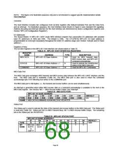
PARALLEL PORT
The LPC47M10x incorporates an IBM XT/AT compatible parallel port. This supports the optional PS/2 type bi-directional
parallel port (SPP), the Enhanced Parallel Port (EPP) and the Extended Capabilities Port (ECP) parallel port modes.
Refer to the Configuration Registers for information on disabling, power down, changing the base address of the parallel
port, and selecting the mode of operation.
The parallel port also incorporates SMSC's ChiProtect circuitry, which prevents possible damage to the parallel port due
to printer power-up.
The functionality of the Parallel Port is achieved through the use of eight addressable ports, with their associated
registers and control gating. The control and data port are read/write by the CPU, the status port is read/write in the EPP
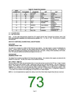
mode. The address map of the Parallel Port is shown below:
DATA PORT
STATUS PORT
BASE ADDRESS + 00H
BASE ADDRESS + 01H
BASE ADDRESS + 02H
BASE ADDRESS + 03H
BASE ADDRESS + 04H
BASE ADDRESS + 05H
BASE ADDRESS + 06H
BASE ADDRESS + 07H
CONTROL PORT
EPP ADDR PORT
EPP DATA PORT 0
EPP DATA PORT 1
EPP DATA PORT 2
EPP DATA PORT 3
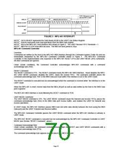
The bit map of these registers is:
D0
PD0
D1
PD1
0
D2
PD2
0
D3
PD3
nERR
SLC
D4
PD4
SLCT
IRQE
D5
PD5
PE
D6
PD6
nACK
0
D7
PD7
nBUSY
0
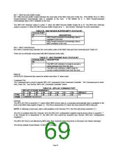
Note
DATA PORT
1
1
1
STATUS PORT TMOUT
CONTROL
PORT
STROBE AUTOFD
nINIT
PCD
EPP ADDR
PORT
EPP DATA
PORT 0
EPP DATA
PORT 1
EPP DATA
PORT 2
PD0
PD0
PD0
PD0
PD0
PD1
PD1
PD1
PD1
PD1
PD2
PD2
PD2
PD2
PD2
PD3
PD3
PD3
PD3
PD3
PD4
PD4
PD4
PD4
PD4
PD5
PD5
PD5
PD5
PD5
PD6
PD6
PD6
PD6
PD6
PD7
PD7
PD7
PD7
PD7
2
2
2
2
2
EPP DATA
PORT 3
Note 1: These registers are available in all modes.
Note 2: These registers are only available in EPP mode.
Page 72

 SMSC [ SMSC CORPORATION ]