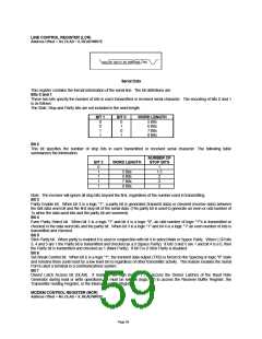
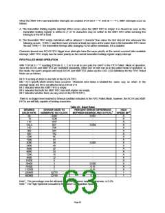
LINE CONTROL REGISTER (LCR)
Address Offset = 3H, DLAB = 0, READ/WRITE
Start LSB Data 5-8 bits MSB Parity Stop
Serial Data
This register contains the format information of the serial line. The bit definitions are:
Bits 0 and 1
These two bits specify the number of bits in each transmitted or received serial character. The encoding of bits 0 and 1
is as follows:
The Start, Stop and Parity bits are not included in the word length.
BIT 1
BIT 0
WORD LENGTH
5 Bits
0
0
1
1
0
1
0
1
6 Bits
7 Bits
8 Bits
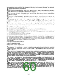
Bit 2
This bit specifies the number of stop bits in each transmitted or received serial character. The following table
summarizes the information.
NUMBER OF
BIT 2
WORD LENGTH
STOP BITS
0
1
1
1
1
-
1
1.5
2
2
2
5 Bits
6 Bits
7 Bits
8 Bits
Note: The receiver will ignore all stop bits beyond the first, regardless of the number used in transmitting.
Bit 3
Parity Enable bit. When bit 3 is a logic "1", a parity bit is generated (transmit data) or checked (receive data) between
the last data word bit and the first stop bit of the serial data. (The parity bit is used to generate an even or odd number of
1s when the data word bits and the parity bit are summed).
Bit 4
Even Parity Select bit. When bit 3 is a logic "1" and bit 4 is a logic "0", an odd number of logic "1"'s is transmitted or
checked in the data word bits and the parity bit. When bit 3 is a logic "1" and bit 4 is a logic "1" an even number of bits is
transmitted and checked.
Bit 5
Stick Parity bit. When parity is enabled it is used in conjunction with bit 4 to select Mark or Space Parity. When LCR bits
3, 4 and 5 are 1 the Parity bit is transmitted and checked as a 0 (Space Parity). If bits 3 and 5 are 1 and bit 4 is a 0, then
the Parity bit is transmitted and checked as 1 (Mark Parity). If bit 5 is 0 Stick Parity is disabled.
Bit 6
Set Break Control bit. When bit 6 is a logic "1", the transmit data output (TXD) is forced to the Spacing or logic "0" state
and remains there (until reset by a low level bit 6) regardless of other transmitter activity. This feature enables the Serial
Port to alert a terminal in a communications system.
Bit 7
Divisor Latch Access bit (DLAB). It must be set high (logic "1") to access the Divisor Latches of the Baud Rate
Generator during read or write operations. It must be set low (logic "0") to access the Receiver Buffer Register, the
Transmitter Holding Register, or the Interrupt Enable Register.
MODEM CONTROL REGISTER (MCR)
Address Offset = 4H, DLAB = X, READ/WRITE
Page 59

 SMSC [ SMSC CORPORATION ]