LPC TRANSFER SEQUENCE EXAMPLES
Wait State Requirements
I/O Transfers
The LPC47M10x inserts three wait states for an I/O read and two wait states for an I/O write cycle. A SYNC of 0110
is used for all I/O transfers. The exception to this is for transfers where IOCHRDY has been deasserted (i.e., EPP or
IrCC transfers) in which case the sync pattern of 0110 is used and a large number of syncs may be inserted (up to
330 which corresponds to a timeout of 10us).
DMA Transfers
The LPC47M10x inserts three wait states for a DMA read and four wait states for a DMA write cycle. A SYNC of
0101 is used for all DMA transfers.
See the example timing for the LPC cycles in the “Timing Diagrams” section.
FLOPPY DISK CONTROLLER
The Floppy Disk Controller (FDC) provides the interface between a host microprocessor and the floppy disk drives. The
FDC integrates the functions of the Formatter/Controller, Digital Data Separator, Write Precompensation and Data Rate
Selection logic for an IBM XT/AT compatible FDC. The true CMOS 765B core guarantees 100% IBM PC XT/AT
compatibility in addition to providing data overflow and underflow protection.
The FDC is compatible to the 82077AA using
SMSC's proprietary floppy disk controller core.
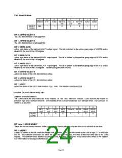
FDC INTERNAL REGISTERS
The Floppy Disk Controller contains eight internal registers which facilitate the interfacing between the host
microprocessor and the disk drive. Table 2 shows the addresses required to access these registers. Registers other
than the ones shown are not supported. The rest of the description assumes that the primary addresses have been
selected.
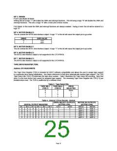
Table 2 - Status, Data and Control Registers
(Shown with base addresses of 3F0 and 370)
PRIMARY
ADDRESS
3F0
SECONDARY
ADDRESS
370
R/W
R
R
R/W
R/W
R
REGISTER
Status Register A (SRA)
Status Register B (SRB)
Digital Output Register (DOR)
Tape Drive Register (TSR)
Main Status Register (MSR)
Data Rate Select Register (DSR)
Data (FIFO)
3F1
3F2
3F3
3F4
3F4
3F5
371
372
373
374
374
375
W
R/W
3F6
376
Reserved
3F7
3F7
377
377
R
W
Digital Input Register (DIR)
Configuration Control Register (CCR)
STATUS REGISTER A (SRA)
Address 3F0 READ ONLY
This register is read-only and monitors the state of the internal interrupt signal and several disk interface pins in PS/2
and Model 30 modes. The SRA can be accessed at any time when in PS/2 mode. In the PC/AT mode the data bus pins
D0 - D7 are held in a high impedance state for a read of address 3F0.
PS/2 Mode
Page 21

 SMSC [ SMSC CORPORATION ]