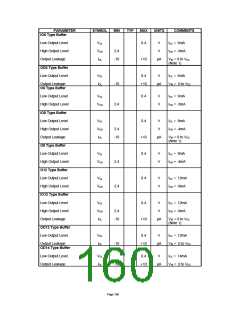
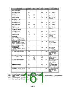
PARAMETER
OP14 Type Buffer
SYMBOL
MIN
TYP
MAX
UNITS
COMMENTS
Low Output Level
High Output Level
Output Leakage
IOP14 Type Buffer
Low Output Level
High Output Level
Output Leakage
IOD16 Type Buffer
Low Output Level
Output Leakage
VOL
VOH
IOL
0.4
V
V
IOL = 14mA
2.4
-10
IOH = -14mA
+10
0.4
µA
VIN = 0 to VCC
(Note 1)
VOL
VOH
IOL
V
V
IOL = 14mA
IOH = -14mA
2.4
-10
+10
µA
VIN = 0 to VCC
(Note 1)
VOL
IOL
IIL
0.4
+10
± 10
V
IOL = 16mA
-10
µA
µA
VIN = 0 to VCC
(Note 1)
VCC = 0V
Backdrive
Protect/ChiProtect
VIN = 5.5V Max
(All pins excluding LAD[3:0],
nLDRQ, nLPCPD, nLFRAME)
5V Tolerant Pins
IIL
± 10
µA
VCC = 3.3V
(All pins excluding LAD[3:0],
nLDRQ, nLPCPD, nLFRAME)
Inputs and Outputs in High
Impedance State
VIN = 5.5V Max
LPC Bus Pins
(LAD[3:0], nLDRQ, nLPCPD,
nLFRAME)
IIL
± 10
153
µA
VCC = 0V and
VCC = 3.3V
VIN = 3.6V Max
All outputs open, all
inputs at a fixed
state (i.e., 0V or
3.3V).
VCC Supply Current Active
ICCI
mA
Trickle Supply Voltage
VTR
VCC
min
VCC
max
V
VCC must not be
greater than .5V
above VTR
All outputs open, all
inputs at a fixed
state (i.e., 0V or
3.3V).
-.5V
VTR Supply Current Active
ITRI
0.253,5
103,4
mA
Reference Voltage
VREF
5.5
13
V
VREF can be either
3.3V (nominal) or
5V (nominal)
All outputs open, all
inputs at a fixed
state (i.e., 0V or
3.3V).
VREF Supply Current Active
IRFI
mA
Note 1: All output leakage’s are measured with all pins in high impedance.
Note 2: Output leakage is measured with the low driving output off, either for a high level output or a high impedance
state.
Note 3: Contact SMSC for the latest values.
Note 4: Max ITRI with VCC = 3.3V (nominal) and CIR ‘on’ is 10 mA.
Page 161

 SMSC [ SMSC CORPORATION ]