The maximum VCC current, ICC, is given with all outputs open (not loaded) and all inputs in a fixed state (i.e., 0V or
3.3V).
The maximum VREF current, IREF, is given with all outputs open (not loaded) and all inputs in a fixed state (i.e., 0V or
3.3V).
Power Management Events (PME/SCI)
The LPC47M10x offers support for Power Management Events (PMEs), also referred to as System Control Interrupt
(SCI) events. The terms PME and SCI are used synonymously throughout this document to refer to the indication of
an event to the chipset via the assertion of the nIO_PME output signal on pin 17. See the “PME Support” section.
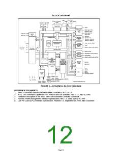
FUNCTIONAL DESCRIPTION
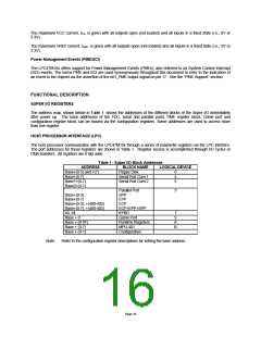
SUPER I/O REGISTERS
The address map, shown below in Table 1, shows the addresses of the different blocks of the Super I/O immediately
after power up. The base addresses of the FDC, serial and parallel ports, PME register block, Game port and
configuration register block can be moved via the configuration registers. Some addresses are used to access more
than one register.
HOST PROCESSOR INTERFACE (LPC)
The host processor communicates with the LPC47M10x through a series of read/write registers via the LPC interface.
The port addresses for these registers are shown in Table 1. Register access is accomplished through I/O cycles or
DMA transfers. All registers are 8 bits wide.
Table 1 - Super I/O Block Addresses
ADDRESS
Base+(0-5) and +(7)
Base+(0-7)
BLOCK NAME
Floppy Disk
Serial Port Com 1
Serial Port Com 2
LOGICAL DEVICE
0
4
5
Base1+(0-7)
Base2+(0-7)
Parallel Port
SPP
3
Base+(0-3)
Base+(0-7)
EPP
Base+(0-3), +(400-402)
Base+(0-7), +(400-402)
60, 64
Base + 0
Base + (0-5F)
Base + (0-7)
ECP
ECP+EPP+SPP
KYBD
Game Port
Runtime Registers
MPU-401
Configuration
7
9
A
B
Base + (0-1)
Note:
Refer to the configuration register descriptions for setting the base address.
Page 16

 SMSC [ SMSC CORPORATION ]