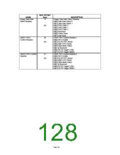
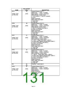
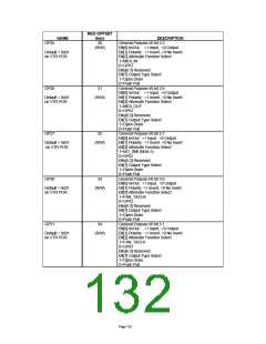
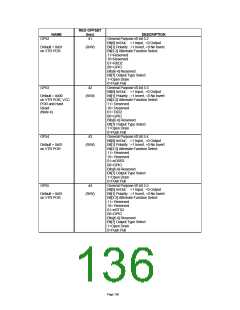
REG OFFSET
(hex)
NAME
DESCRIPTION
General Purpose I/0 bit 2.5
GP25
30
(R/W)
Bit[0] In/Out : =1 Input, =0 Output
Bit[1] Polarity : =1 Invert, =0 No Invert
Bit[2] Alternate Function Select
1=MIDI_IN
Default = 0x01
on VTR POR
0=GPIO
Bits[6:3] Reserved
Bit[7] Output Type Select
1=Open Drain
0=Push Pull
GP26
31
General Purpose I/0 bit 2.6
Bit[0] In/Out : =1 Input, =0 Output
Bit[1] Polarity : =1 Invert, =0 No Invert
Bit[2] Alternate Function Select
1=MIDI_OUT
Default = 0x01
on VTR POR
(R/W)
0=GPIO
Bits[6:3] Reserved
Bit[7] Output Type Select
1=Open Drain
0=Push Pull
GP27
32
General Purpose I/0 bit 2.7
Bit[0] In/Out : =1 Input, =0 Output
Bit[1] Polarity : =1 Invert, =0 No Invert
Bit[2] Alternate Function Select
1=nIO_SMI (Note 5)
0=GPIO
Default = 0x01
on VTR POR
(R/W)
Bits[6:3] Reserved
Bit[7] Output Type Select
1=Open Drain
0=Push Pull
GP30
33
General Purpose I/0 bit 3.0
Bit[0] In/Out : =1 Input, =0 Output
Bit[1] Polarity :=1 Invert, =0 No Invert
Bit[2] Alternate Function Select
1=FAN_TACH2
Default = 0x01
on VTR POR
(R/W)
0=GPIO
Bits[6:3] Reserved
Bit[7] Output Type Select
1=Open Drain
0=Push Pull
GP31
34
General Purpose I/0 bit 3.1
Bit[0] In/Out : =1 Input, =0 Output
Bit[1] Polarity : =1 Invert, =0 No Invert
Bit[2] Alternate Function Select
1=FAN_TACH1
Default = 0x01
on VTR POR
(R/W)
0=GPIO
Bits[6:3] Reserved
Bit[7] Output Type Select
1=Open Drain
0=Push Pull
Page 132

 SMSC [ SMSC CORPORATION ]