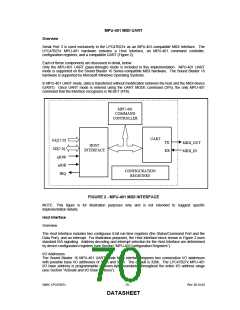
INFRARED INTERFACE
The infrared interface provides a two-way wireless communications port using infrared as a transmission
medium. Several IR implementations have been provided for the second UART in this chip (logical device
5), IrDA, Consumer Remote Control, and Amplitude Shift Keyed IR. The IR transmission can use the
standard UART2 TXD2 and RXD2 pins or optional IRTX2 and IRRX2 pins. These can be selected through
the configuration registers.
IrDA 1.0 allows serial communication at baud rates up to 115.2 kbps. Each word is sent serially beginning
with a zero value start bit. A zero is signaled by sending a single IR pulse at the beginning of the serial bit
time. A one is signaled by sending no IR pulse during the bit time. Please refer to the AC timing for the
parameters of these pulses and the IrDA waveform.
The consumer remote control interface can decode NEC PPM remote control frames in hardware as well
provide a general-purpose synchronous ASK encoder/decoder with programmable carrier frequency and
bit rates to emulate many other popular remote control encoding formats; including 38 kHz PPM, PWM
and RC-5. Consult the SMSC CIrCC data sheet for more details.
The Amplitude Shift Keyed IR allows asynchronous serial communication at baud rates up to 19.2K Baud.
Each word is sent serially beginning with a zero value start bit. A zero is signaled by sending a 500kHz
waveform for the duration of the serial bit time. A one is signaled by sending no transmission during the bit
time. Please refer to the AC timing for the parameters of the ASK-IR waveform.
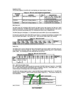
If the Half Duplex option is chosen, there is a time-out when the direction of the transmission is changed.
This time-out starts at the last bit transferred during a transmission and blocks the receiver input until the
timeout expires. If the transmit buffer is loaded with more data before the time-out expires, the timer is
restarted after the new byte is transmitted. If data is loaded into the transmit buffer while a character is
being received, the transmission will not start until the time-out expires after the last receive bit has been
received. If the start bit of another character is received during this time-out, the timer is restarted after the
new character is received. The IR half duplex time-out is programmable via CRF2 in Logical Device 5.
This register allows the time-out to be programmed to any value between 0 and 10msec in 100usec
increments.
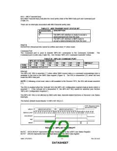
IR Transmit Pins
The following description pertains to the TXD2 and IRTX2 pins of the LPC47B27x.
Following a VTR POR, the TXD2 and IRTX2 pins will be output and low. They will remain low until one
of the following conditions are met:
IRTX2/GP35 Pin. This pin defaults to the IRTX2 function.
1. This pin will remain low following a VCC POR until serial port 2 is enabled by setting the activate
bit, at which time the pin will reflect the state of the IR transmit output of the IRCC block.
2. This pin will remain low following a VCC POR until the GPIO output function is selected for the pin,
at which time the pin will reflect the state of the GPIO data bit if it is configured as an output.
GP53/TXD2 Pin. This pin defaults to the GPIO output function.
1. This pin will remain low following a VCC POR until the TXD2 function is selected for the pin AND
serial port 2 is enabled by setting the activate bit, at which time the pin will reflect the state of the IR
transmit output of the IRCC block (if IR is enabled through the IR Options Register for Serial Port 2)
2. This pin will remain low following a VCC POR until the TXD2 function is selected for the pin AND
serial port 2 is enabled by setting the activate bit, at which time the pin will reflect the state of the
transmit output of serial port 2
3. This pin will remain low following a VCC POR until the corresponding GPIO data bit (GP5 register
bit 3) is set or the polarity bit in the GP53 control register is set.
SMSC LPC47B27x
- 69 -
Rev. 08-10-04
DATASHEET

 SMSC [ SMSC CORPORATION ]