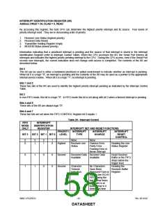
MODEM STATUS REGISTER (MSR)
Address Offset = 6H, DLAB = X, READ/WRITE
This 8 bit register provides the current state of the control lines from the MODEM (or peripheral device). In addition to
this current state information, four bits of the MODEM Status Register (MSR) provide change information. These bits are
set to logic "1" whenever a control input from the MODEM changes state. They are reset to logic "0" whenever the
MODEM Status Register is read.
Bit 0
Delta Clear To Send (DCTS). Bit 0 indicates that the nCTS input to the chip has changed state since the last time the
MSR was read.
Bit 1
Delta Data Set Ready (DDSR). Bit 1 indicates that the nDSR input has changed state since the last time the MSR was
read.
Bit 2
Trailing Edge of Ring Indicator (TERI). Bit 2 indicates that the nRI input has changed from logic "0" to logic "1".
Bit 3
Delta Data Carrier Detect (DDCD). Bit 3 indicates that the nDCD input to the chip has changed state.
Note: Whenever bit 0, 1, 2, or 3 is set to a logic "1", a MODEM Status Interrupt is generated.
Bit 4
This bit is the complement of the Clear To Send (nCTS) input. If bit 4 of the MCR is set to logic "1", this bit is equivalent
to nRTS in the MCR.
Bit 5
This bit is the complement of the Data Set Ready (nDSR) input. If bit 4 of the MCR is set to logic "1", this bit is
equivalent to DTR in the MCR.
Bit 6
This bit is the complement of the Ring Indicator (nRI) input. If bit 4 of the MCR is set to logic "1", this bit is equivalent to
OUT1 in the MCR.
Bit 7
This bit is the complement of the Data Carrier Detect (nDCD) input. If bit 4 of the MCR is set to logic "1", this bit is
equivalent to OUT2 in the MCR.
SCRATCHPAD REGISTER (SCR)
Address Offset =7H, DLAB =X, READ/WRITE
This 8 bit read/write register has no effect on the operation of the Serial Port. It is intended as a scratchpad register to
be used by the programmer to hold data temporarily.
PROGRAMMABLE BAUD RATE GENERATOR (AND DIVISOR LATCHES DLH, DLL)
The Serial Port contains a programmable Baud Rate Generator that is capable of dividing the PLL clock by any
divisor from 1 to 65535. The internal PLL clock is divided down to generate a 1.8462MHz frequency for Baud Rates
less than 38.4k, a 1.8432MHz frequency for 115.2k, a 3.6864MHz frequency for 230.4k and a 7.3728MHz frequency
for 460.8k. This output frequency of the Baud Rate Generator is 16x the Baud rate. Two 8 bit latches store the
divisor in 16 bit binary format. These Divisor Latches must be loaded during initialization in order to insure desired
operation of the Baud Rate Generator. Upon loading either of the Divisor Latches, a 16 bit Baud counter is
immediately loaded. This prevents long counts on initial load. If a 0 is loaded into the BRG registers the output
divides the clock by the number 3. If a 1 is loaded the output is the inverse of the input oscillator. If a two is loaded
the output is a divide by 2 signal with a 50% duty cycle. If a 3 or greater is loaded the output is low for 2 bits and high
for the remainder of the count.
Table 30 shows the baud rates.
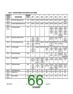
Effect Of The Reset on Register File
The Reset Function (Table 31) details the effect of the Reset input on each of the registers of the Serial Port.
SMSC LPC47B27x
- 62 -
Rev. 08-10-04
DATASHEET

 SMSC [ SMSC CORPORATION ]