Three Port 10/100 Managed Ethernet Switch with MII
Datasheet
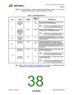
Table 3.8 Miscellaneous Pins
BUFFER
PIN
NAME
SYMBOL
TYPE
DESCRIPTION
General
Purpose I/O
Data
GPIO[11:8]
IS/OD12/ General Purpose I/O Data: These general
purpose signals are fully programmable as either
push-pull outputs, open-drain outputs, or Schmitt-
triggered inputs by writing the General Purpose I/O
Configuration Register (GPIO_CFG) and General
Purpose I/O Data & Direction Register
O12
(PU)
Note 3.14
77-79,
82
(GPIO_DATA_DIR). For more information, refer to
Chapter 12, "GPIO/LED Controller," on page 142.
Note:
The remaining GPIO[7:0] pins share
functionality with the LED output pins, as
described in Table 3.1 and Table 3.2.
Interrupt
Output
IRQ
O8/OD8
Interrupt Output: Interrupt request output. The
polarity, source and buffer type of this signal is
programmable via the Interrupt Configuration
Register (IRQ_CFG). For more information, refer to
Chapter 5, "System Interrupts," on page 52.
63
71
SystemReset
Input
nRST
IS
(PU)
System Reset Input: This active low signal allows
external hardware to reset the LAN9313/LAN9313i.
The LAN9313/LAN9313i also contains an internal
power-on reset circuit. Thus, this signal may be left
unconnected if an external hardware reset is not
needed. When used, this signal must adhere to the
reset timing requirements as detailed in Section
14.5.2, "Reset and Configuration Strap Timing," on
page 390.
Test 1
Test 2
TEST1
TEST2
AI
AI
Test 1: This pin must be tied to VDD33IO for
75
proper operation.
Test 2: This pin must be tied to VDD33IO for
proper operation.
108
Note 3.14 The input buffers are enabled when configured as GPIO inputs only.
Table 3.9 PLL Pins
BUFFER
TYPE
PIN
NAME
SYMBOL
DESCRIPTION
PLL +1.8V
Power Supply
VDD18PLL
P
PLL +1.8V Power Supply: This pin must be
connected to VDD18CORE for proper operation.
107
Refer to the LAN9313/LAN9313i application note
for additional connection information.
Crystal Input
XI
ICLK
Crystal Input: External 25MHz crystal input. This
signal can also be driven by a single-ended clock
oscillator. When this method is used, XO should be
left unconnected.
105
106
Crystal
Output
XO
OCLK
Crystal Output: External 25MHz crystal output.
SMSC LAN9313/LAN9313i
Revision 1.2 (04-08-08)
DATA3S9HEET

 SMSC [ SMSC CORPORATION ]