High-Performance Single-Chip 10/100 Ethernet Controller with HP Auto-MDIX
Datasheet
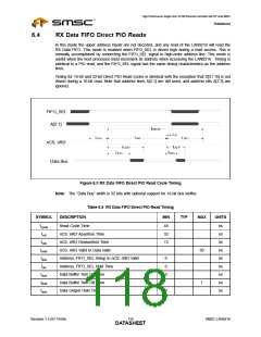
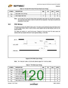
Note: An RX Data FIFO Direct PIO Read cycle begins when both nCS and nRD are asserted. The
cycle ends when either or both nCS and nRD are de-asserted. They may be asserted and de-
asserted in any order.
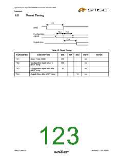
6.5
RX Data FIFO Direct PIO Burst Reads
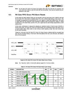
In this mode the upper address inputs are not decoded, and any burst read of the LAN9218 will read
the RX Data FIFO. This mode is enabled when FIFO_SEL is driven high during a read access. This
is normally accomplished by connecting the FIFO_SEL signal to a high-order address line. This mode
is useful when the host processor must increment its address when accessing the LAN9218. Timing
is identical to a PIO Burst Read, and the FIFO_SEL signal has the same timing characteristics as the
address lines.
In this mode, performance is improved by allowing an unlimited number of back-to-back DWORD or
WORD read cycles. RX Data FIFO Direct PIO Burst Reads can be performed using Chip Select (nCS)
or Read Enable (nRD). When either or both of these control signals go high, they must remain high
for the period specified.
Timing for 16-bit and 32-bit RX Data FIFO Direct PIO Burst Reads is identical with the exception that
D[31:16] are not driven during a 16-bit burst. Note that address lines A[2:1] are still used, and address
bits A[7:3] are ignored.
FIFO_SEL
A[2:1]
nCS, nRD
Data Bus
Figure 6.4 RX Data FIFO Direct PIO Burst Read Cycle Timing
Note: The “Data Bus” width is 32 bits with optional support for 16-bit bus widths.
Table 6.6 RX Data FIFO Direct PIO Burst Read Cycle Timing
SYMBOL
DESCRIPTION
MIN
TYP
MAX
UNITS
tcsh
tcsdv
tacyc
tasu
tadv
tah
nCS, nRD Deassertion Time
nCS, nRD Valid to Data Valid
Address Cycle Time
13
ns
ns
30
45
0
Address, FIFO_SEL Setup to nCS, nRD Valid
Address Stable to Data Valid
Address, FIFO_SEL Hold Time
Data Buffer Turn On Time
ns
40
0
0
ns
ns
tdon
SMSC LAN9218
119
Revision 1.5 (07-18-06)
DATASHEET

 SMSC [ SMSC CORPORATION ]