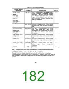
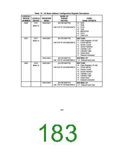
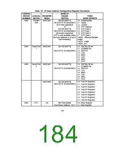
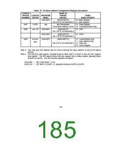
Table 78 - I/O Base Address Configuration Register Description
BASE I/O
LOGICAL
DEVICE LOGICAL REGISTER
RANGE
(NOTE3)
FIXED
BASE OFFSETS
NUMBER DEVICE
INDEX
0x62,0x63
[0x100:0xFFE]
+0: Index Register
ON 2 BYTE BOUNDARIES +1: Data Register
Not Relocatable +0 : Data Register
Fixed Base Address: 60,64 +4 : Command/Status Reg.
0x07
0x08
KYBD
n/a
Aux. I/O
0x60,0x61
0x62,0x63
0x60,0x61
[0x00:0xFFF]
+0 : GPR
ON 1 BYTE BOUNDARIES
[0x00:0xFFF]
+0 : GPW
ON 1 BYTE BOUNDARIES
0x09
Access.
Bus
[0x00:0x0FFC]
+0 : Control/Status Reg
+1 : Own Address Reg
ON 4 BYTE BOUNDARIES +2 : Data Reg
+3 : Clock Register
Note 3: This chip uses ISA address bits [A11:A0] to decode the base address of each of its logical
devices.
Note 4: The IDE/FDC split register, normally found at either 0x3F7 or 0x377 is now an FDC support
only register. The IDE logical Device will now support only a status register (typically found
at 0x3F6 or 0x376). The IDE Decoder operates as follows:
nHDCS0# = IDE TASK BASE + [7:0]
nHDCS1# = IDE MISC AT BASE + 0 (typically located at 0x3F6 or 0x376)
185

 SMSC [ SMSC CORPORATION ]