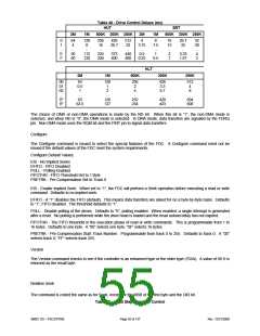
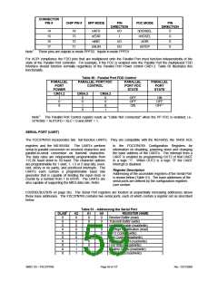
CONNECTOR
PIN #
CHIP PIN #
SPP MODE
PIN
FDC MODE
PIN
DIRECTION
DIRECTION
14
15
16
17
74
73
72
71
nAFD
nERR
nINIT
nSLIN
I/O
I
I/O
I/O
nDENSEL
nHDSEL
nDIR
0
0
0
0
nSTEP
Note1: These pins are outputs in mode PPFD2. Inputs in mode PPFD1
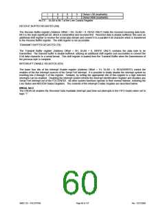
For ACPI compliance the FDD pins that are multiplexed onto the Parallel Port must function independently of the
state of the Parallel Port controller. For example, if the FDC is enabled onto the Parallel Port the multiplexed FDD
Interface should function normally regardless of the Parallel Port Power control CR01.2. Table 50 illustrates this
functionality.
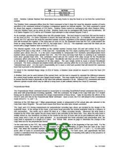
Table 50 - Parallel Port FDD Control
PARALLEL
PARALLEL PORT FDC
CONTROL
PARALLEL
PORT FDC
STATE
PARALLEL
PORT
PORT
POWER
STATE
CR01.2
CR04.3
CR04.2
1
0
X
0
0
1
X
0
0
X
1
OFF
OFF
ON
ON
OFF
OFF1
Note1: The Parallel Port Control register reads as “Cable Not Connected” when the PP FDC is enabled; i.e.,
STROBE = AUTOFD = SLC = 0 and nINIT = 1.
SERIAL PORT (UART)
The FDC37N769 incorporates two full function UARTs. They are compatible with the NS16450, the 16450 ACE
registers and the NS16550A. The UARTs perform
serial-to-parallel conversion on received characters and
parallel-to-serial conversion on transmit characters.
The data rates are independently programmable from
115.2K baud down to 50 baud. The character options
are programmable for 1 start; 1, 1.5 or 2 stop bits; even,
odd, sticky or no parity; and prioritized interrupts. The
to the FDC37N769 Configuration Registers for
information on disabling, powering down and changing
the base address of the UARTs. The interrupt from a
UART is enabled by programming OUT2 of that UART
to a logic “1”. When OUT2 is a logic “0” the UART
Interrupt is disabled.
Register Description
UARTs each contain
a programmable baud rate
Addressing of the accessible registers of the Serial Port
is shown below (Table 51). The base addresses of the
serial ports are defined by the configuration registers
(see section
generator that is capable of dividing the input clock or
crystal by a number from 1 to 65535. The UARTs are
also capable of supporting the MIDI data rate. Refer
CONFIGURATION on page 96). The Serial Port registers are located at sequentially increasing addresses above
these base addresses. The FDC37N769 contains two serial ports, each of which contain a register set as described
below.
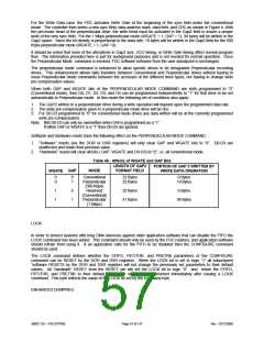
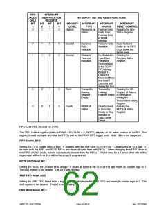
Table 51 - Addressing the Serial Port
DLAB1
A2
0
A1
0
A0
0
REGISTER NAME
0
0
Receive Buffer (read)
0
0
0
Transmit Buffer (write)
0
0
0
1
Interrupt Enable (read/write)
Interrupt Identification (read)
FIFO Control (write)
Line Control (read/write)
Modem Control (read/write)
Line Status (read/write)
Modem Status (read/write)
Scratchpad (read/write)
X
X
X
X
X
X
X
0
1
0
0
1
0
0
1
1
1
0
0
1
0
1
1
1
0
1
1
1
SMSC DS – FDC37N769
Page 59 of 137
Rev. 12/21/2000

 SMSC [ SMSC CORPORATION ]