During powerdown accessing FDC registers that do not affect the power state may increase device power
consumption, but only until the register access has been completed.
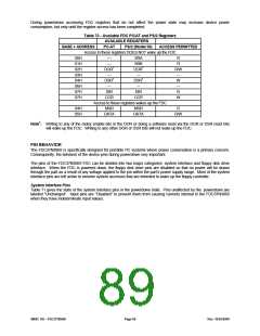
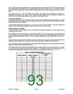
Table 70 - Available FDC PC/AT and PS/2 Registers
AVAILABLE REGISTERS
BASE + ADDRESS
PC-AT
PS/2 (Model 30)
ACCESS PERMITTED
Access to these registers DOES NOT wake up the FDC
00H
01H
02H
03H
04H
06H
07H
07H
----
----
SRA
SRB
DOR1
---
R
R
R/W
---
W
---
R
W
DOR1
---
DSR1
---
DIR
CCR
DSR1
---
DIR
CCR
Access to these registers wakes up the FDC
04H
05H
MSR
DATA
MSR
DATA
R
R/W
Note1: Writing to any of the motor enable bits in the DOR or doing a software reset via the DOR or DSR reset bits
will wake up the FDC. Writing to any other DOR or DSR bits will not wake up the FDC.
PIN BEHAVIOR
The FDC37N3869 is specifically designed for portable PC systems where power conservation is a primary concern.
Consequently, the behavior of the device pins during powerdown very important.
The pins of the FDC37N3869 FDC can be divided into two major categories: system interface and floppy disk drive
interface. When the FDC is powered down, the floppy disk drive pins are disabled so that no power will be drawn
through the part as a result of any voltage applied to the pin within the part’s power supply range. Most of the system
interface pins are left active to monitor system accesses that are intended to wake up the floppy controller.
System Interface Pins
Table 71 gives the state of the system interface pins in the powerdown state. Pins unaffected by the powerdown are
labeled “Unchanged”. Input pins are “Disabled” to prevent them from causing currents internal to the FDC37N3869
when they have indeterminate input values.
SMSC DS – FDC37N3869
Page 89
Rev. 10/25/2000

 SMSC [ SMSC CORPORATION ]