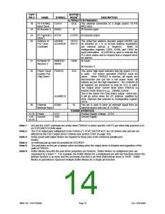
TQFP
PIN #
BUFFER
NAME
SYMBOL
MODE6
DESCRIPTION
ALTERNATE IR PINS/MISC
18
23
24
92
14.318 MHz
Input Clock
IR Receive 2 IRRX2
CLK14
ICLK
The external connection to a single source 14.318
MHz clock.
IS
IR Receive input
IR Transmit 2 IRTX2
(Note5)
Address X/
PCI Clock
Controller
O12PD IR transmit output
nADRX/
OD12/ The active-low address decoder output nADRX can
IOD12 be asserted on 1, 8, or 16-byte address boundaries
nCLKRUN
(an external pull-up is required).
Refer to
configuration registers CR03, CR08, and CR09 for
more information. nCLKRUN is used to indicate the
PCI clock status and to request that a stopped clock
be started.
21
56
IR Mode/ IR
Receive 3
IRMODE/
IRRX3
O6/IS
I/O4
IR mode
IR Receive 3
Power Good/ PWRGD
nGame Port
This active high input indicates that the power (VCC)
is valid. For device operation PWRGD must be
active. When PWRGD is inactive, all inputs are
disconnected and put into a low power mode; all
outputs are put into high impedance. The contents of
all registers are preserved as long as VCC is valid.
The output driver current drain when PWRGD is
inactive mode drops to ISTBY - standby current.
This is the Game Port Chip Select output - active low.
It will go active when the I/O address, qualified by
AEN, matches that selected in Configuration register
CR1E.
Chip Select
nGAMECS
96
External
IRQIN
IS
This pin is used to steer an interrupt signal from an
external device onto one of 15 IRQs.
Interrupt Input
POWER INTERFACE
Positive Supply Voltage. (3.3V)
Ground Supply.
13,70 Power
4,45, Ground
65,93
VCC
VSS
Note 1: nRI and the UART interrupts are active when PWRGD is active and the UARTS are either fully powered or in
AUTOPOWER DOWN mode.
Note 2: The FDD output pins multiplexed in the PARALLEL PORT INTERFACE are OD drivers only and are not
affected by the FDD Output Driver Controls (see section CR05 on page 102).
Note 3: Active (push-pull) output drivers are required on these pins in the enhanced parallel port
modes.
Note 4: An external pull-up must be provided for IOCHRDY.
Note 5: The pull-down on this pin is always active including when the output driver is tristated and regardless of the
state of PWRGD.
Note 6: Buffer Modes describe the pad driver properties per function. Buffer Modes on multiplexed pins are
separated by a slash “/”. For example, the Buffer Modes for a multiplexed pin with two functions where the
primary function is an input and the secondary function is an 8mA bidirectional driver is “I/IO8”. Buffer
Modes in parenthesis represent multiple Buffer Modes for a single pin function.
SMSC DS – FDC37N3869
Page 14
Rev. 10/25/2000

 SMSC [ SMSC CORPORATION ]