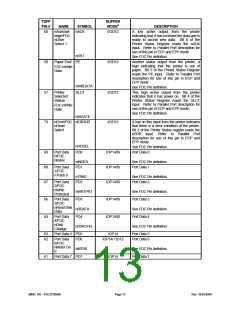
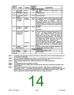
FUNCTIONAL DESCRIPTION
Super I/O Registers
Table 3 shows the addresses of the various device blocks of the Super I/O immediately after power up. The base
addresses must be set in the configuration registers before accessing these devices. The base addresses of the FDC,
Serial and Parallel Ports can be moved via the configuration registers.
Host Processor Interface
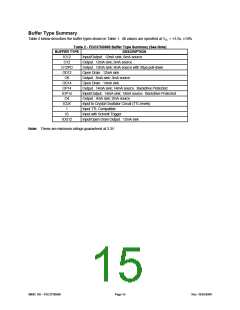
The host processor communicates with the FDC37N3869 using the Super I/O registers. Register access is
accomplished through programmed I/O or DMA transfers. All registers are 8 bits wide. All host interface output
buffers are capable of sinking a minimum of 12 mA.
Table 3 - FDC37N3869 Block Addresses
ADDRESS
3F0, 3F1 or 370, 371
Base +[0:7]
Base +[0:7]
Base1 +[0:7]
Base2 +[0:7]
BLOCK NAME
Configuration
NOTES
Write only; Note 1
Floppy Disk
Serial Port Com 1
Serial Port Com 2
Disabled at power up; Note 2
Disabled at power up; Note 2
Disabled at power up; Note 2
Base +[0:3] all modes
Base +[4:7] for EPP
Base +[400:403] for ECP
Parallel Port
Disabled at power up; Note 2
Note 1: Configuration registers can only be modified in the configuration state, refer to section CONFIGURATION on
page 96 for more information. All logical blocks in the FDC37N3869 can operate normally in the Configuration State.
Note 2: The base addresses must be set in the configuration registers before accessing device blocks.
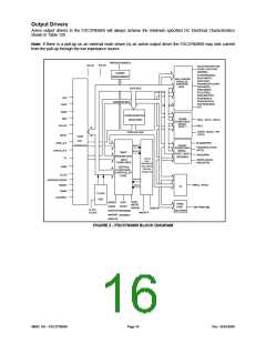
FLOPPY DISK CONTROLLER
The Floppy Disk Controller (FDC) provides the interface between a host microprocessor and the floppy disk drives.
The FDC integrates the functions of the Formatter/Controller, Digital Data Separator, Write Precompensation and
Data Rate Selection logic for an IBM XT/AT compatible FDC. The true CMOS 765B core guarantees 100% IBM PC
XT/AT compatibility in addition to providing data overflow and underflow protection.
The FDC37N3869 is compatible with the 82077AA using SMSC’s proprietary floppy disk controller core. For
information about the floppy disk on the Parallel Port pins refer to section Parallel Port Floppy Disk Controller on page
54.
Modes Of Operation
The FDC37N3869 Floppy Disk Controller has two Floppy modes and three Interface modes. Each of the three
Interface modes are available in each of the two Floppy modes.
FLOPPY MODES
The Floppy modes are used to select alternate configurations for the Tape Drive register. The active Floppy mode is
determined by the Enhanced Floppy Mode 2 bit in Configuration Register 3 (see section CR03 on page 100). When
the Enhanced Floppy Mode 2 bit is 0 Normal Floppy mode is selected, otherwise Enhanced Floppy Mode 2 (OS/2
mode) is selected. See section TAPE DRIVE REGISTER (TDR) on page 24 for the affects of the Enhanced Floppy
Mode 2 bit on the Tape Drive register.
SMSC DS – FDC37N3869
Page 17
Rev. 10/25/2000

 SMSC [ SMSC CORPORATION ]