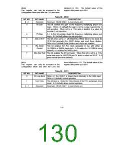
initialized to 1EH. The default value of this
register after power up is 80H. This register is
used to select the base address of the Game
Chip Select decoder (GAMECS). The GAMECS
can be set to 48 locations, on 16 byte
boundaries from 100H-3F0H. To disable the
GAMECS, set DB1 and DB0 to zero.
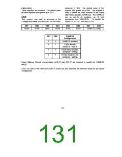
CR12-CR1D
These registers are reserved. The default value
of these registers after power up is 00H.
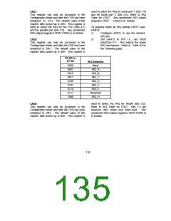
CR1E
This register can only be accessed in the
Configuration Mode and after the CSR has been
DB7
DB6
DB5
DB4
DB3
DB2
DB1
DB0
ADR9
ADR8
ADR7
ADR6
ADR5
ADR4
GAMECS Config
DB1
DB0
GAMECS
Configuration
0
0
0
1
GAMECS disabled
1 Byte decode,
ADR[3:0] = 0001b
1
1
0
1
8 Byte block decode,
ADR[3:0] = 0XXXb
16 byte block decode,
ADR[3:0] = XXXXb
Upper Address Decode requirements: nCS='0' and A10='0' are required to qualify the GAMECS
output.
CR03, bit DB0 is the PWRGD/GAMECS control bit and overrides the selection made by the above
configuration.
131

 SMSC [ SMSC CORPORATION ]