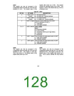
of this register after power up is 00H. This
register indicates the Drive Type used for each
drive. Refer to CR0B for Data Rate Table
register.
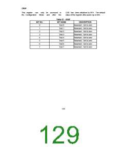
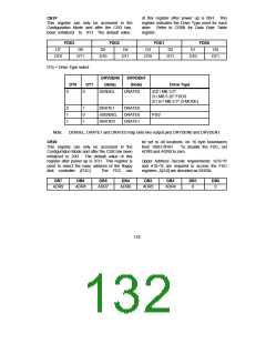
CR1F
This register can only be accessed in the
Configuration Mode and after the CSR has
been initialized to 1FH. The default value
FDD3
FDD2
FDD1
FDD0
D7
D6
D5
D4
D3
D2
D1
D0
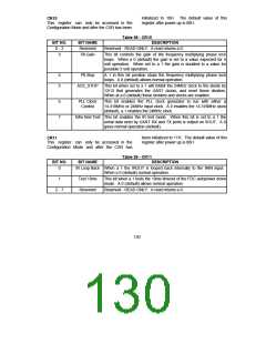
DT0
DT1
DT0
DT1
DT0
DT1
DT0
DT1
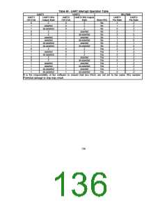
DTx = Drive Type select
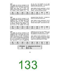
DRVDEN0
(Note)
DRVDEN1
DT0
DT1
(Note)
Drive Type
0
0
DENSEL
DRATE0
4/2/1 MB 3.5"
2/1 MB 5.25" FDDS
2/1.6/1 MB 3.5" (3-MODE)
0
1
1
1
0
1
DRATE1
nDENSEL
DRATE0
DRATE0
DRATE0
DRATE1
PS/2
Note:
CR20
DENSEL, DRATE1 and DRATE0 map onto two output pins DRVDEN0 and DRVDEN1.
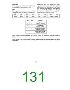
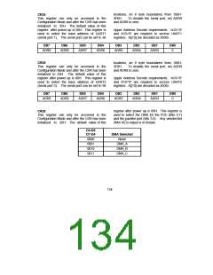
be set to 48 locations, on 16 byte boundaries
This register can only be accessed in the
Configuration Mode and after the CSR has been
initialized to 20H. The default value of this
register after power up is 3CH. This register is
used to select the base address of the floppy
from 100H-3F0H.
ADR9 and ADR8 to zero.
To disable the FDC, set
Upper Address Decode requirements: nCS='0'
and A10='0' are required to access the FDC
registers. A[3:0] are decoded as 0XXXb.
disk controller (FDC).
The FDC can
DB7
DB6
DB5
ADR7
DB4
DB3
DB2
DB1
DB0
ADR9
ADR8
ADR6
ADR5
ADR4
0
0
132

 SMSC [ SMSC CORPORATION ]