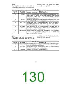
initialized to 10H. The default value of this
register after power up is 00H.
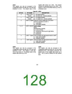
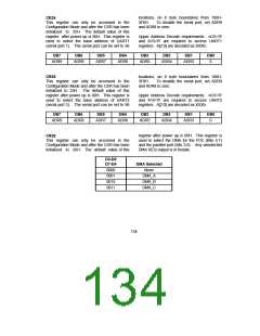
CR10
This register can only be accessed in the
Configuration Mode and after the CSR has been
Table 58 - CR10
BIT NO.
0 - 2
3
BIT NAME
Reserved
Pll Gain
DESCRIPTION
Reserved - READ ONLY. A read returns a 0.
This bit controls the gain of the frequency multiplying phase lock
loops. When a 0 (default) the gain is set to a value expected for 5
volt operation. When set to a 1 the gain is doubled to a value for
possible 3 volt operation.
4
5
Pll Stop
A 1 in this bit position stops the frequency multiplying phase lock
loops. A 0 (default) allows normal operation.
ACE_STOP
This bit when set to a 1 will inhibit the 24MHz clock to the divide by
12/13 that generates the UART clocks, and reset those dividers.
When at a 0 (default) these dividers and clocks are enabled.
6
7
PLL Clock
Control
This bit enables the PLL clock generator to run with either a
14.318MHz or 24MHz input clock. A 0 enables the 14.318MHz clock
(default), a 1 enables the 24MHz clock.
Infra Red Test This bit enables the IR test mode. When this bit is set to a 1 the
serial data seen by UART RX and TX ports is output on SOUT. A 0
gives normal operation (default).
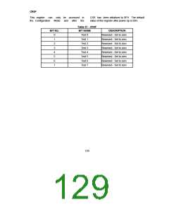
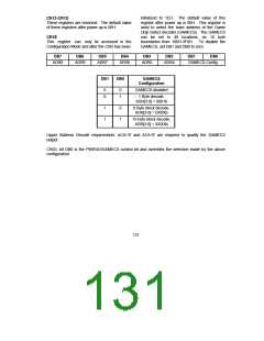
been initialized to 11H. The default value of this
CR11
This register can only be accessed in the
register after power up is 00H.
Configuration Mode and after the CSR has
Table 59 - CR11
DESCRIPTION
BIT NO.
BIT NAME
0
IR Loop Back When a 1 the IROUT is looped back internally to the IRIN input.
When a 0 (default) normal operation.
1
Test 10ms
This bit when a 1 tests the 10ms timeout of the FDC autopower down
mode. A 0 (default) allows normal operation.
2 - 7
Reserved
Reserved - READ ONLY. A read returns a 0.
130

 SMSC [ SMSC CORPORATION ]