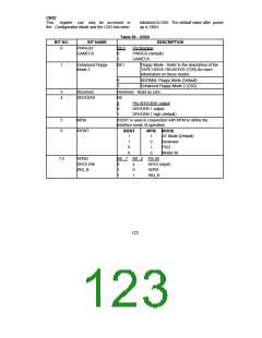
CR08
CR09
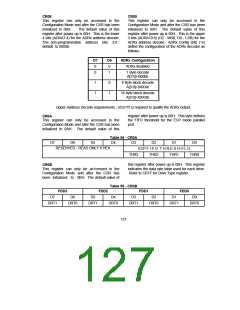
This register can only be accessed in the
Configuration Mode and after the CSR has been
This register can only be accessed in the
Configuration Mode and after the CSR has been
initialized to 09H. The default value of this
register after power up is 00H. This is the upper
3 bits (ADRA10:8) (D2 - MSB, D0 - LSB) for the
ADRx address decode. ADRx Config (bits 7:6)
define the configuration of the ADRx decoder as
follows:
initialized to 08H.
The default value of this
register after power up is 00H. This is the lower
4 bits (ADRA7:4) for the ADRx address decode.
The non-programmable address bits 3:0
default to 0000b.
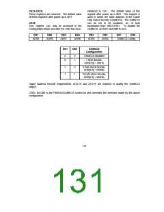
D7
0
D6
0
ADRx Configuration
ADRx disabled
0
1
1 Byte decode
A[3:0]=0000b
1
1
0
1
8 Byte block decode
A[3:0]=0XXXb
16 byte block decode
A[3:0]=XXXXb
Upper Address Decode requirements : nCS='0' is required to qualify the ADRx output.
register after power up is 00H. This byte defines
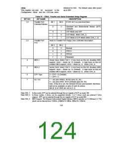
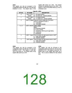
CR0A
This register can only be accessed in the
Configuration Mode and after the CSR has been
initialized to 0AH. The default value of this
the FIFO threshold for the ECP mode parallel
port.
Table 54 - CR0A
D4 D3
D7
D6
D5
D2
ECP F I F O T H R E S H O L D
THR3 THR2 THR1
D1
D0
RESERVED - READ ONLY 0 HEX
THR0
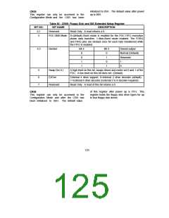
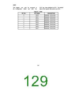
this register after power up is 00H. This register
indicates the data rate table used for each drive.
Refer to CR1F for Drive Type register.
CR0B
This register can only be ac1cessed in the
Configuration Mode and after the CSR has
been initialized to 0BH. The default value of
Table 55 - CR0B
FDD3
FDD2
FDD1
FDD0
D7
D6
D5
D4
D3
D2
D1
D0
DRT1
DRT0
DRT1
DRT0
DRT1
DRT0
DRT1
DRT0
127

 SMSC [ SMSC CORPORATION ]