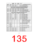
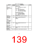
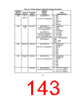
Table 54 - Chip Level Registers
DESCRIPTION
REGISTER
OSC
ADDRESS
STATE
0x24 R/W Bit[0] Reserved
Bit [1] PLL Control
C
Default = 0x04, on
Vcc POR or
Reset_Drv hardware
signal.
= 0
= 1
PLL is on (backward Compatible)
PLL is off
Bits[3:2] OSC
= 01
= 10
= 00
= 11
Osc is on, BRG clock is on.
Same as above (01) case.
Osc is on, BRG Clock Enabled.
Osc is off, BRG clock is disabled.
Bit [5:4] Reserved, set to zero
Bit [6] 16-Bit Address Qualification
= 0
= 1
12-Bit Address Qualification
16-Bit Address Qualification
Bit[7] Reserved
Chip Level
Vendor Defined
0x25
0x26
Reserved - Writes are ignored, reads return 0.
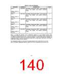
Bit[7:1] Configuration Address Bits [7:1]
Bit[0] = 0
See Note 1
Configuration
Address Byte 0
C
C
Default
=0xF0 (Sysopt=0)
=0x70 (Sysopt=1)
on Vcc POR or
Reset_Drv
Configuration
Address Byte 1
0x27
0x28
Bit[7:0] Configuration Address Bits [15:8]
See Note 1
Default = 0x03
on Vcc POR or
Reset_Drv
Default = 0x00
on VCC POR and
Hard Reset
Bits[7:0] Reserved - Writes are ignored, reads
return 0.
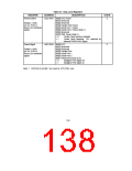
Chip Level
0x29 -0x2A Reserved - Writes are ignored, reads return 0.
Vendor Defined
139

 SMSC [ SMSC CORPORATION ]