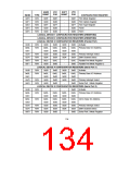
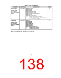
Table 53 - Chip Level Registers
DESCRIPTION
REGISTER
ADDRESS
STATE
PowerControl
0x22 R/W Bit[0] FDC Power
Bit[1] Reserved
C
Default = 0x00.
on Vcc POR or
Reset_Drv hardware
signal
Bit[2] Reserved
Bit[3] Parallel Port Power
Bit[4] Serial Port 1 Power
Bit[5] Serial Port 2 Power (Note 1)
Bit[6] Reserved
Bit[7] PME Power (Note 1)
= 0
= 1
Trickle Clock Inactive (default)
Trickle Clock Running. PLL selected by
internal PWRGOOD signal.
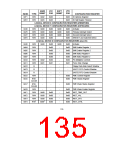
Power Mgmt
0x23 R/W Bit[0] FDC
Bit[1] Reserved
C
Default = 0x00.
on Vcc POR or
Reset_Drv hardware
signal
Bit[2] Reserved
Bit[3] Parallel Port
Bit[4] Serial Port 1
Bit[5] Serial Port 2
Bit[6:7] Reserved (read as 0)
= 0
= 1
Intelligent Pwr Mgmt off
Intelligent Pwr Mgmt on
Note 1: CR22 Bit 5 and Bit 7 are reset by VTR POR, only.
138

 SMSC [ SMSC CORPORATION ]