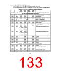
Table 53 - Chip Level Registers
DESCRIPTION
REGISTER
ADDRESS
STATE
Index Address
0x03 R/W Bit[7]
= 1
Enable WDT_CTRL and SMI Enable and
SMI Status Register access when not in
configuration mode
Default = 0x03
= 0
Disable WDT_CTRL and SMI Enable and
SMI Status Register access when not in
configuration mode (Default)
on Vcc POR or
Reset_Drv
Bits [6:2]
Reserved - Writes are ignored, reads return 0.
Bits[1:0]
Sets GP index register address when in Run mode
(not in Configuration Mode).
= 11 0xEA (Default)
= 10 0xE4
= 01 0xE2
= 00 0xE0
0x04 - 0x06
Reserved - Writes are ignored, reads return 0.
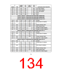
Logical Device #
0x07 R/W A write to this register selects the current logical
device. This allows access to the control and
configuration registers for each logical device.
Note: The Activate command operates only on the
selected logical device.
C
Default = 0x00
on Vcc POR or
Reset_Drv
Card Level
Reserved
0x08 - 0x1F
Reserved - Writes are ignored, reads return 0.
Chip Level, SMSC Defined
Device ID
0x20 R
A
read only register which provides device
C
C
identification. Bits[7:0] = 0x43 when read.
Hard wired
= 0x43
Device Rev
0x21 R
A read only register which provides device revision
information. Bits[7:0] = current revision when read.
Hard wired
= Current Revision
137

 SMSC [ SMSC CORPORATION ]