Fan Control Device with High Frequency PWM Support and Hardware Monitoring Features
Datasheet
Note: SMSC Test Registers may be read/write registers. Writing these registers can cause unwanted
results.
Note 8.1 The PWMx Current Duty Cycle Registers are only writable when the associated fan is in
manual mode. In this case, the register is writable when the start bit is set, but not when
the lock bit is set.
Note 8.2 The Lock bit in the Ready/Lock/Start register is locked by the Lock Bit. The START and
OVRID bits are always writable, both when the start bit is set and when the lock bit is set.
Note 8.3 The Interrupt status registers are cleared on a read if no events are active
Note 8.4 The INTEN bit in register 7Ch is always writable, both when the start bit is set and when
the lock bit is set.
Note 8.5 In Shutdown Mode (LPMD=1 & START=0) all the H/W Monitoring registers/bits are not
accessible except for the following: Bits[2:0] in the Special Function Register (SFTR) at
offset 7Ch and Bits[7:0] in the Configuration register at offset 7Fh.
Note 8.6 These Reserved bits are read/write bits. Writing these bits to a ‘1’ has no effect on the
hardware.
Note 8.7 SMSC bits may be read/write bits. Writing these bits to a value other than the default value
may cause unwanted results
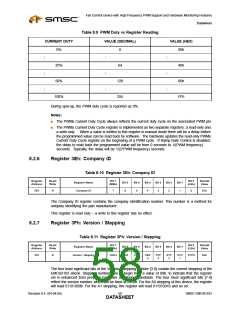
8.1
Undefined Registers
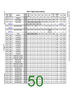
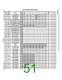
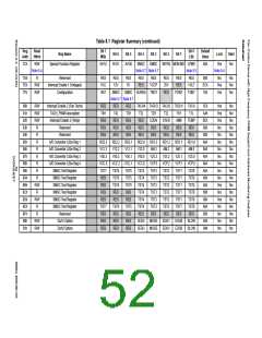
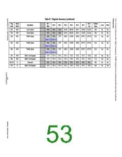
The registers shown in Table 8.1, "Register Summary" above are the defined registers in the part. Any
reads to undefined registers always return 00h. Writes to undefined registers have no effect and do
not return an error.
8.2
Defined Registers
8.2.1
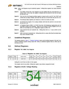
Register 10h: SMSC Test Register
Table 8.2 Register 10h: SMSC Test Register
Register
Address
Read/
Write
Bit 7
Bit 0
Default
Value
Register Name
Bit 6
Bit 5
Bit 4
Bit 3
Bit 2
Bit 1
(MSb)
(LSb)
10h
R/W
SMSC TEST
TST7
TST6
TST5
TST4
TST3
TST2
TST1
TST0
00h
Setting the Lock bit has no effect on this register.
This register must not be written. Writing this register may produce unexpected results.
8.2.2
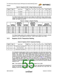
Registers 20-24h: Voltage Reading
Table 8.3 Registers 20-24h: Voltage Reading
Register
Address
Read/
Write
Bit 7
Bit 0
Default
Value
Register Name
Bit 6
Bit 5
Bit 4
Bit 3
Bit 2
Bit 1
(MSb)
(LSb)
20h
21h
R
R
+2.5V Reading
Vccp Reading
7
7
6
6
5
5
4
4
3
3
2
2
1
1
0
0
N/A
N/A
Revision 0.4 (04-04-05)
SMSC EMC6D103
DATA5S4HEET

 SMSC [ SMSC CORPORATION ]