Legacy-Free Keyboard/Embedded Controller with SPI and LPC Docking Interface
Chapter 1 General Description
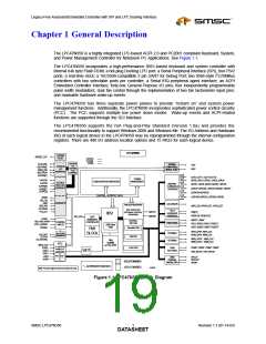
The LPC47N350 is a highly integrated LPC-based ACPI 2.0 and PC2001 compliant Keyboard, System,
and Power Management Controller for Notebook PC Applications. See Figure 1.1.
The LPC47N350 incorporates a high-performance 8051-based keyboard and system controller with
internal 64k byte Flash ROM; a hot-plug Docking LPC port; a Serial Peripheral Interface (SPI), four PS/2
ports; a real-time clock; a 16C550A-compatible 2 pin UART for Debug Port; two 8584-style I2C/SMBus
controllers with two selectable ports per controller; a Serial IRQ peripheral agent interface; an ACPI
Embedded Controller Interface; forty-one General Purpose I/O pins; four independently programmable
pulse width modulators; dual fan control through the implementation of two fan tachometer input pins;
and maskable hardware wake-up events.
The LPC47N350 has three separate power planes to provide “instant on” and system power
management functions. Additionally, the LPC47N350 incorporates sophisticated power control circuitry
(PCC). The PCC supports multiple low power down modes. Wake-up events and ACPI-related
functions are supported through the SCI Interface.
The LPC47N350 supports the ISA Plug-and-Play Standard (Version 1.0a) and provides the
recommended functionality to support Windows 2000 and Windows Me. The I/O Address and Hardware
IRQ of each logical device in the LPC47N350 may be reprogrammed through the internal configuration
registers. There are 480 I/O address location options and 15 IRQ’s for each logical device.
LPC47N350
SYSTEM
nRESET_OUT
RESET
VCC1(5)
VCC2(3)
VSS(8)
DOCKING
LPC
DLAD[3:0]
nDLFRAME
DSER_IRQ
nDCLKRUN
nDLDRQ[1]
16C550A
TXD*
RXD*
DOCKING
LPC
COMPATIBLE
SERIAL PORT
BUFFERS
AND
INTERFACE
CONTROL
OUT
I/O
OUT0, OUT1*, (OUT7-OUT11)*
GPIO0, GPIO1, GPIO2*, GPIO3, GPIO4*
GPIO5*, GPIO6, (GPIO7-GPIO9)*, GPIO10
POWER
LAD [3:0]
CONFIGURATION REGISTERS
CONTROL, ADDRESS, DATA
MANAGEMENT
LPC BUS
HOST CPU
INTERFACE
nLPCPD
GENERAL
I/O
nLFRAME
PURPOSE I/O
INTERFACE
I/O
I/O
I/O
(GPIO11-GPIO18)*, GPIO19, GPIO20*, GPIO21*
(SGPIO30-SGPIO33)*
nLRESET
nLDRQ[1]
LGPIO50-LGPIO53, LGPIO60-LGPIO63
nIRQ8*
nEC_SCI
nSMI*
SER_IRQ
nCLKRUN
PCI_CLK
INTERRUPTS
LED DRIVER
MAILBOX REGISTERS
nBAT_LED, nPWR_LED*, nFDD_LED*
8051 SUB-BLOCK
EXTERNAL CONTROL
REGISTERS
16 x 8
8051TX*
8051RX*
KSI[0:7]
KSO[0:13], KSO[14:15]*
KEYBOARD
INTERFACE
8051
nEC_SCI
ACPI
MODE
nEA, PGM, nFWP
VCC1_PWRGD
EMBEDDED
CONTROLLER
KBRST*, A20M*
KCLK, EMCLK, IMCLK, PS2CLK*
KDAT, EMDAT, IMDAT, PS2DAT*
EXTERNAL
8051 RAM
CONTROL
INPUTS
PS/2 PORTS
256B Direct
RAM
PWRGD
Executable RAM
PM1
AB1A_DATA, AB1A_CLK
AB1B_DATA, AB1B_CLK
I2C/SMBus
I2C/SMBus
PLL CLOCK
BLOCK
CLK_OUT
CLOCKI
GENERATOR
Data RAM
AB2A_DATA *, AB2A_CLK *
AB2B_DATA *, AB2B_CLK *
(14.318 MHz)
Ring
Oscillator
RTC
32kHz_OUT
XOSEL
XTAL2
w/ FAIL SAFE
2 x 128 BYTE
BANKS OF
CMOS RAM
PWM0*, PWM1*, PWM2*, PWM3*
FAN_TACH1*, FAN_TACH2*
FLASH ROM
PWM
Fan Control
WDT
XTAL1
BANK BANK
VCC0
Serial
SPCLK*
SPDOUT*
SPDIN*
1
2
AGND
Peripheral
VCC2 POWERED
Interface (SPI)
* -- ALTERNATE FUNCTION
VCC1 POWERED
3-26-02
Note: The block diagram should not used for pin count.
Figure 1.1 LPC47N350 Block Diagram
SMSC LPC47N350
1
Revision 1.1 (01-14-03)
DATASHEET

 SMSC [ SMSC CORPORATION ]