ST7781
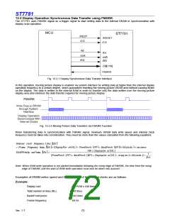
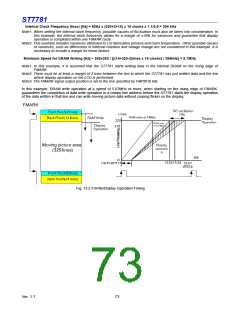
Internal Clock Frequency (fosc) [Hz] = 60Hz x (320+2+14) x 16 clocks x 1.1/0.9 = 394 kHz
Note1. When setting the internal clock frequency, possible causes of fluctuation must also be taken into consideration. In
this example, the internal clock frequency allows for a margin of ±10% for variances and guarantee that display
operation is completed within one FMARK cycle.
Note2. This example includes variances attributed to LSI fabrication process and room temperature. Other possible causes
of variances, such as differences in external resistors and voltage change are not considered in this example. It is
necessary to include a margin for these factors.
Minimum Speed for DRAM Writing [Hz] > 240x320 / {((14+320-2)lines x 16 clocks) / 394kHz} = 5.7MHz
Note1. In this example, it is assumed that the ST7781 starts writing data in the internal DRAM on the rising edge of
FMARK.
Note2. There must be at least a margin of 2 lines between the line to which the ST7781 has just written data and the line
where display operation on the LCD is performed.
Note3. The FMARK signal output position is set to the line specified by FMP[8:0] bits.
In this example, DRAM write operation at a speed of 5.67MHz or more, when starting on the rising edge of FMARK,
guarantees the completion of data write operation in a certain line address before the ST7781 starts the display operation
of the data written in that line and can write moving picture data without causing flicker on the display.
Fig. 13.2.3 Write/Display Operation Timing
Ver. 1.7
73

 SITRONIX [ SITRONIX TECHNOLOGY CO., LTD. ]