ST7781
12. Reset Function
The ST7781 is initialized by the RESET input. During reset period, the ST7781 is in a busy state and instruction from the
MCU and DRAM access are not accepted. The ST7781’s internal power supply circuit unit is initialized also by the RESET
input. The RESET period must be secured for at least 1ms. In case of power-on reset, wait until the RC oscillation
frequency stabilizes (for 1 ms). During this period, DRAM access and initial instruction setting are prohibited.
12.1. Initial State of Instruction Bits (Default)
See the Instruction desscription.The default value is shown in the parenthesis of each instruction bit cell.
12.2. RAM Data Initialization
The RAM data is not automatically initialized by the RESET input. It must be initialized by software in display-off
period.
12.3. Note on Reset Function
(1) When a RESET input is entered into the ST7781 while it is in deep standby mode, the ST7781 starts up the inside
logic regulator and makes a transition to the initial state. During this period, the state of the interface pins may
become unstable. For this reason, do not enter a RESET input in deep standby mode.
(2) When transferring instruction in either two or three transfers via 8-/9-/16-bit interface, make sure to execute data
transfer synchronization after reset operation.
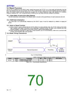
12.4 Reset Timing Characterics
Fig. 12.4 Reset timing
VDDI=1.65 to 3.3V, VDD=2.5 to 3.3V, AGND=DGND=0V, Ta=25
℃
Signal
Symbol
TRESL
TREST
Parameter
Reset Low Level Width
Reset Complete Time
Min
1
1
Max
-
Unit
ms
ms
Description
RESET
-
Table 12.4.1: Reset timing Characteristics
Ver. 1.7
70

 SITRONIX [ SITRONIX TECHNOLOGY CO., LTD. ]