SiI 1160 PanelLink Transmitter
Data Sheet
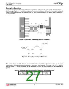
Decoupling Capacitors
Designers should include decoupling and bypass capacitors at each power pin in the layout. These are shown
schematically in Figure 15. Place these components as close as possible to the PanelLink device pins, and avoid
routing through vias if possible, as shown in Figure 14, which is representative of the various types of power pins
on the transmitter.
VCC
L1
C1
C2
VCC
GND
Ferrite
C3
Via to GND
Figure 14. Decoupling and Bypass Capacitor Placement
VCC
L1
VCCPIN
C1
C2
C3
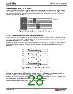
Figure 15. Decoupling and Bypass Schematic
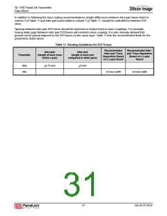
The values shown in Table 10 are recommendations that should be adjusted according to the noise
characteristics of the specific board-level design. Pins in one group (such as IVCC) may share C2, L1, and C3,
each pin having C1 placed as close to the pin as possible. PGND1 and PGND2 should be tied individually to
ground.
Table 10. Recommended Components for Bypass and Decoupling Circuits
C1
C2
C3
L1
100 – 300 pF
2.2 – 10 uF
10 uF
200+ Ω
23
SiI-DS-0126-B

 SILICONIMAGE [ Silicon image ]