EFR32MG13 Mighty Gecko Multi-Protocol Wireless SoC Family Data Sheet
Electrical Specifications
Parameter
Note:
Symbol
Test Condition
Min
Typ
Max
Unit
1. Specified configuration for Unit gain buffer configuration is: INCBW = 0, HCMDIS = 0, RESINSEL = DISABLE. VINPUT = 0.5 V,
VOUTPUT = 0.5 V.
2. Specified configuration for 3X-Gain configuration is: INCBW = 1, HCMDIS = 1, RESINSEL = VSS, VINPUT = 0.5 V, VOUTPUT = 1.5
V. Nominal voltage gain is 3.
3. If the maximum CLOAD is exceeded, an isolation resistor is required for stability. See AN0038 for more information.
4. Current into the load resistor is excluded. When the OPAMP is connected with closed-loop gain > 1, there will be extra current to
drive the resistor feedback network. The internal resistor feedback network has total resistance of 143.5 kOhm, which will cause
another ~10 µA current when the OPAMP drives 1.5 V between output and ground.
5. In unit gain connection, UGF is the gain-bandwidth product of the OPAMP. In 3x Gain connection, UGF is the gain-bandwidth
product of the OPAMP and 1/3 attenuation of the feedback network.
6. Step between 0.2V and VOPA-0.2V, 10%-90% rising/falling range.
7. When INCBW is set to 1 the OPAMP bandwidth is increased. This is allowed only when the non-inverting close-loop gain is ≥ 3,
or the OPAMP may not be stable.
8. From enable to output settled. In sample-and-off mode, RC network after OPAMP will contribute extra delay. Settling error < 1mV.
9. When HCMDIS=1 and input common mode transitions the region from VOPA-1.4V to VOPA-1V, input offset will change. PSRR
and CMRR specifications do not apply to this transition region.
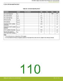
4.1.22 Pulse Counter (PCNT)
Table 4.53. Pulse Counter (PCNT)
Parameter
Symbol
Test Condition
Min
Typ
Max
Unit
Input frequency
FIN
Asynchronous Single and Quad-
rature Modes
—
—
10
MHz
Sampled Modes with Debounce
filter set to 0.
—
—
8
kHz
4.1.23 Analog Port (APORT)
Table 4.54. Analog Port (APORT)
Parameter
Symbol
Test Condition
Min
—
Typ
7
Max
—
Unit
µA
Supply current1 2
IAPORT
Operation in EM0/EM1
Operation in EM2/EM3
—
63
—
nA
Note:
1. Supply current increase that occurs when an analog peripheral requests access to APORT. This current is not included in repor-
ted peripheral currents. Additional peripherals requesting access to APORT do not incur further current.
2. Specified current is for continuous APORT operation. In applications where the APORT is not requested continuously (e.g. peri-
odic ACMP requests from LESENSE in EM2), the average current requirements can be estimated by mutiplying the duty cycle of
the requests by the specified continuous current number.
silabs.com | Building a more connected world.
Rev. 1.4 | 107

 SILICON [ SILICON ]