C8051F52x-53x
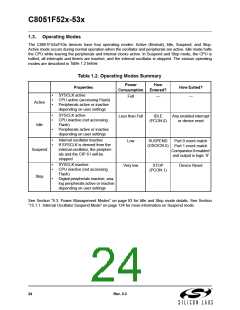
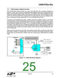
1.4. 12-Bit Analog to Digital Converter
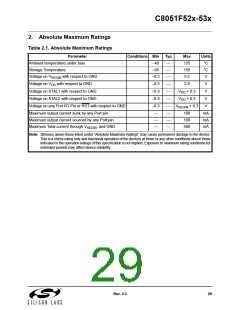
The C8051F52x/F53x devices include an on-chip 12-bit SAR ADC with a maximum throughput of
200 ksps. The ADC system includes a configurable analog multiplexer that selects the positive ADC input,
which is measured with respect to GND. Ports 0 and 1 are available as ADC inputs; additionally, the ADC
includes an innovative half gain selection which allows for inputs up to twice the Vref voltage to be sam-
pled. The on-chip Temperature Sensor output and the core supply voltage (V ) are also available as ADC
DD
inputs. User firmware may shut down the ADC or use it in Burst Mode to save power.
Conversions can be initiated in three ways: a software command, an overflow of Timer 2 or an external
convert start signal. This flexibility allows the start of conversion to be triggered by software events, a peri-
odic signal (timer overflows), or external HW signals. Conversion completions are indicated by a status bit
and an interrupt (if enabled) and occur after 1, 4, 8, or 16 samples have been accumulated by a hardware
accumulator. The resulting 12-bit to 16-bit data word is latched into the ADC data SFRs upon completion of
a conversion. When the system clock is slow, Burst Mode allows ADC0 to automatically wake from a low
power shutdown state, acquire and accumulate samples, then re-enter the low power shutdown state with-
out CPU intervention.
Window compare registers for the ADC data can be configured to interrupt the controller when ADC data is
either within or outside of a specified range. The ADC can monitor a key voltage continuously in back-
ground mode, but not interrupt the controller unless the converted data is within/outside the specified
range.
Analog Multiplexer
Configuration, Control, and Data Registers
P0.0
AD0BUSY (W)
Start
Conversion
CNVSTR Rising Edge
P0.6*
P0.7*
P1.0*
Burst Mode
Logic
Timer 2 Overflow
P1.7*
19-to-1
AMUX
12-Bit
SAR
* Available in
‘F53x parts
ADC Data
Registers
16
ADC
Accumulator
Temp
Sensor
Window
Compare
Interrupt
VDD
GND
Window Compare
Logic
End of
Conversion
Interrupt
Figure 1.5. 12-Bit ADC Block Diagram
Rev. 0.3
25

 SILICON [ SILICON ]