C8051F52x-53x
ging. All the peripherals (except for the ADC) are stalled when the MCU is halted, during single stepping,
or at a breakpoint in order to keep them synchronized.
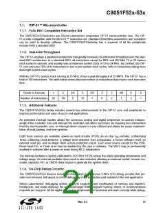
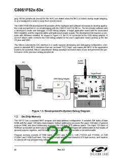
The C8051F530-DK development kit provides all the hardware and software necessary to develop applica-
tion code and perform in-circuit debugging with the C8051F52x/F53x MCUs. The kit includes software with
a developer's studio and debugger, a USB debug adapter, a target application board with the associated
MCU installed, and the required cables and wall-mount power supply. The development kit requires a com-
puter with Windows installed. As shown in Figure 1.3, the PC is connected to the USB debug adapter. A
six-inch ribbon cable connects the USB debug adapter to the user's application board, picking up the two
C2 pins and GND.
The Silicon Laboratories IDE interface is a vastly superior developing and debugging configuration, com-
pared to standard MCU emulators that use on-board "ICE Chips" and require the MCU in the application
board to be socketed. Silicon Laboratories’ debug paradigm increases ease of use and preserves the per-
formance of the precision analog peripherals.
AC/DC
Adapter
PC
Target Board
P1
HDR2
RESET_B
USB Debug Adapter
J7
J4
USB
Cable
J3
J5
TB2
HDR3
HDR1
Figure 1.3. Development/In-System Debug Diagram
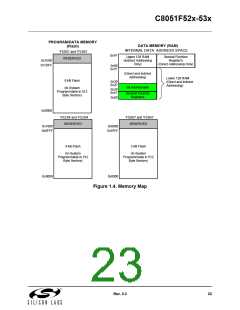
1.2. On-Chip Memory
The CIP-51 has a standard 8051 program and data address configuration. It includes 256 bytes of data
RAM, with the upper 128 bytes dual-mapped. Indirect addressing accesses the upper 128 bytes of general
purpose RAM, and direct addressing accesses the 128 byte SFR address space. The lower 128 bytes of
RAM are accessible via direct and indirect addressing. The first 32 bytes are addressable as four banks of
general purpose registers, and the next 16 bytes can be byte addressable or bit addressable.
Program memory consists of 7680 bytes (‘F520/1 and ‘F530/1), 4 kB (‘F523/4 and ‘F533/4), or 2 kB
(‘F526/7 and ‘F536/7) of Flash. This memory is byte writable and erased in 512-byte sectors, and requires
no special off-chip programming voltage.
22
Rev. 0.3

 SILICON [ SILICON ]