C8051F52x-53x
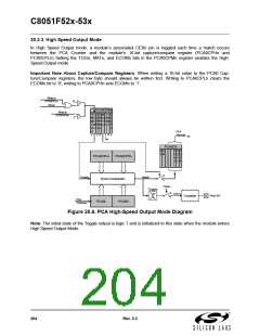
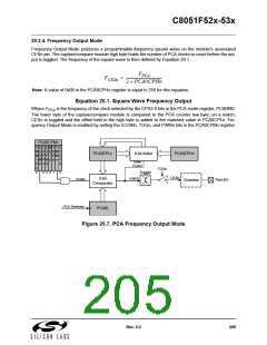
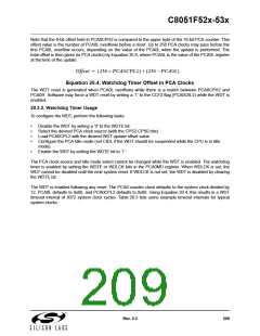
20.2.4. Frequency Output Mode
Frequency Output Mode produces a programmable-frequency square wave on the module’s associated
CEXn pin. The capture/compare module high byte holds the number of PCA clocks to count before the out-
put is toggled. The frequency of the square wave is then defined by Equation 20.1.
FPCA
----------------------------------------
=
FCEXn
2 × PCA0CPHn
Note: A value of 0x00 in the PCA0CPHn register is equal to 256 for this equation.
Equation 20.1. Square Wave Frequency Output
Where F
is the frequency of the clock selected by the CPS2-0 bits in the PCA mode register, PCA0MD.
PCA
The lower byte of the capture/compare module is compared to the PCA counter low byte; on a match,
CEXn is toggled and the offset held in the high byte is added to the matched value in PCA0CPLn. Fre-
quency Output Mode is enabled by setting the ECOMn, TOGn, and PWMn bits in the PCA0CPMn register.
PCA0CPMn
P
W
M
1
6
n
E C C M T
C A A A O
O P P T G
M P N n n
n n n
P
W
M
n
E
C
C
F
n
PCA0CPLn
8-bit Adder
PCA0CPHn
Adder
Enable
TOGn
0
0 0 0 1
0
Toggle
0
CEXn
8-bit
Comparator
match
Enable
Crossbar
Port I/O
1
PCA Timebase
PCA0L
Figure 20.7. PCA Frequency Output Mode
Rev. 0.3
205

 SILICON [ SILICON ]