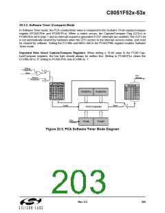
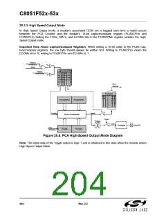
C8051F52x-53x
20.2. Capture/Compare Modules
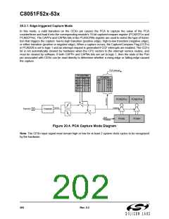
Each module can be configured to operate independently in one of six operation modes: Edge-triggered
Capture, Software Timer, High Speed Output, Frequency Output, 8-Bit Pulse Width Modulator, or 16-Bit
Pulse Width Modulator. Each module has Special Function Registers (SFRs) associated with it in the CIP-
51 system controller. These registers are used to exchange data with a module and configure the module's
mode of operation.
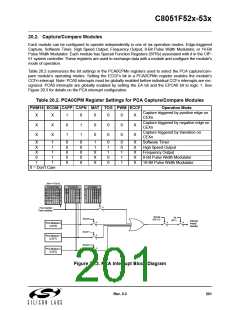
Table 20.2 summarizes the bit settings in the PCA0CPMn registers used to select the PCA capture/com-
pare module’s operating modes. Setting the ECCFn bit in a PCA0CPMn register enables the module's
CCFn interrupt. Note: PCA0 interrupts must be globally enabled before individual CCFn interrupts are rec-
ognized. PCA0 interrupts are globally enabled by setting the EA bit and the EPCA0 bit to logic 1. See
Figure 20.3 for details on the PCA interrupt configuration.
Table 20.2. PCA0CPM Register Settings for PCA Capture/Compare Modules
PWM16 ECOM CAPP CAPN MAT TOG PWM ECCF
Operation Mode
Capture triggered by positive edge on
CEXn
Capture triggered by negative edge on
CEXn
X
X
X
X
X
X
1
0
1
0
1
1
0
0
0
0
0
0
0
0
0
X
X
X
Capture triggered by transition on
CEXn
X
X
X
0
1
1
1
1
1
0
0
0
0
0
0
0
0
0
0
1
1
X
X
X
0
1
1
0
0
0
0
1
1
1
X
X
X
X
X
Software Timer
High Speed Output
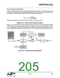
Frequency Output
8-Bit Pulse Width Modulator
16-Bit Pulse Width Modulator
1
X = Don’t Care
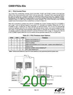
(for n = 0 to 5)
PCA0CPMn
PCA0CN
C C C
PCA0MD
P E C C M T P E
W C A A A O W C
M O P P T G M C
1 M P N n n n F
C C
F R
C
I
D
L
C C C E
C C C
F F F
2 1 0
P P P C
S S S F
2 1 0
6 n n n
n
n
0
1
PCA Counter/
Timer Overflow
EPCA0
(EIE1.4)
EA
(IE.7)
ECCF0
ECCF1
ECCF2
Interrupt
Priority
Decoder
0
1
0
1
0
1
PCA Module 0
(CCF0)
0
1
PCA Module 1
(CCF1)
0
1
PCA Module 2
(CCF2)
Figure 20.3. PCA Interrupt Block Diagram
Rev. 0.3
201

 SILICON [ SILICON ]