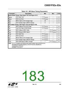
C8051F52x-53x
19.1.2. Mode 1: 16-bit Counter/Timer
Mode 1 operation is the same as Mode 0, except that the counter/timer registers use all 16 bits. The
counter/timers are enabled and configured in Mode 1 in the same manner as for Mode 0.
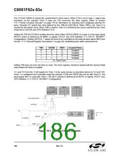
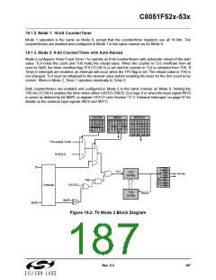
19.1.3. Mode 2: 8-bit Counter/Timer with Auto-Reload
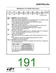
Mode 2 configures Timer 0 and Timer 1 to operate as 8-bit counter/timers with automatic reload of the start
value. TL0 holds the count and TH0 holds the reload value. When the counter in TL0 overflows from all
ones to 0x00, the timer overflow flag TF0 (TCON.5) is set and the counter in TL0 is reloaded from TH0. If
Timer 0 interrupts are enabled, an interrupt will occur when the TF0 flag is set. The reload value in TH0 is
not changed. TL0 must be initialized to the desired value before enabling the timer for the first count to be
correct. When in Mode 2, Timer 1 operates identically to Timer 0.
Both counter/timers are enabled and configured in Mode 2 in the same manner as Mode 0. Setting the
TR0 bit (TCON.4) enables the timer when either GATE0 (TMOD.3) is logic 0 or when the input signal /INT0
is active as defined by bit IN0PL in register IT01CF (see Section “11.5. External Interrupts” on page 97 for
details on the external input signals /INT0 and /INT1).
CKCON
TMOD
INT01CF
G C T T G C T T
I I I I I I I I
T T T T S S
2 2 1 0 C C
MMMM A A
A
/
1 1 A
/
0 0
N N N N N N N N
1 1 1 1 0 0 0 0
P S S S P S S S
L L L L L L L L
T T M M T T M M
E 1 1 0 E 0 1 0
H L
1 0
1
0
2 1 0
2 1 0
Pre-scaled Clock
SYSCLK
0
1
0
1
T0
TF1
TR1
TF0
TR0
IE1
TCLK
TL0
(8 bits)
Interrupt
TR0
IT1
IE0
IT0
Crossbar
GATE0
TH0
Reload
(8 bits)
IN0PL
XOR
/INT0
Figure 19.2. T0 Mode 2 Block Diagram
Rev. 0.3
187

 SILICON [ SILICON ]