C8051F52x-53x
19. Timers
Each MCU includes three counter/timers: two are 16-bit counter/timers compatible with those found in the
standard 8051, and one is a 16-bit auto-reload timer for use with other device peripherals or for general
purpose use. These timers can be used to measure time intervals, count external events and generate
periodic interrupt requests. Timer 0 and Timer 1 are nearly identical and have four primary modes of oper-
ation. Timer 2 offer 16-bit and split 8-bit timer functionality with auto-reload.
Timer 0 and Timer 1 Modes:
13-bit counter/timer
Timer 2 Modes:
16-bit timer with auto-reload
16-bit counter/timer
8-bit counter/timer with auto-reload
Two 8-bit counter/timers
(Timer 0 only)
Two 8-bit timers with auto-reload
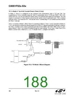
Timers 0 and 1 may be clocked by one of five sources, determined by the Timer Mode Select bits (T1M–
T0M) and the Clock Scale bits (SCA1–SCA0). The Clock Scale bits define a pre-scaled clock from which
Timer 0 and/or Timer 1 may be clocked (See SFR Definition 19.3 for pre-scaled clock selection).
Timer 0/1 may then be configured to use this pre-scaled clock signal or the system clock. Timer 2 may be
clocked by the system clock, the system clock divided by 12, or the external oscillator clock source divided
by 8.
Timer 0 and Timer 1 may also be operated as counters. When functioning as a counter, a counter/timer
register is incremented on each high-to-low transition at the selected input pin (T0 or T1). Events with a fre-
quency of up to one-fourth the system clock's frequency can be counted. The input signal need not be peri-
odic, but it must be held at a given level for at least two full system clock cycles to ensure the level is
properly sampled.
19.1. Timer 0 and Timer 1
Each timer is implemented as a 16-bit register accessed as two separate bytes: a low byte (TL0 or TL1)
and a high byte (TH0 or TH1). The Counter/Timer Control register (TCON) is used to enable Timer 0 and
Timer 1 as well as indicate status. Timer 0 interrupts can be enabled by setting the ET0 bit in the IE register
(Section “11.4. Interrupt Register Descriptions” on page 93); Timer 1 interrupts can be enabled by setting
the ET1 bit in the IE register (Section 11.4). Both counter/timers operate in one of four primary modes
selected by setting the Mode Select bits T1M1–T0M0 in the Counter/Timer Mode register (TMOD). Each
timer can be configured independently. Each operating mode is described below.
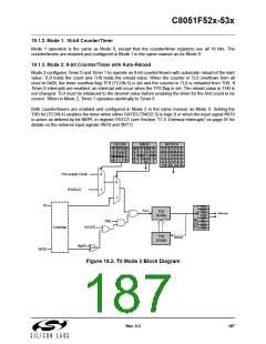
19.1.1. Mode 0: 13-bit Counter/Timer
Timer 0 and Timer 1 operate as 13-bit counter/timers in Mode 0. The following describes the configuration
and operation of Timer 0. However, both timers operate identically, and Timer 1 is configured in the same
manner as described for Timer 0.
The TH0 register holds the eight MSBs of the 13-bit counter/timer. TL0 holds the five LSBs in bit positions
TL0.4–TL0.0. The three upper bits of TL0 (TL0.7–TL0.5) are indeterminate and should be masked out or
ignored when reading. As the 13-bit timer register increments and overflows from 0x1FFF (all ones) to
0x0000, the timer overflow flag TF0 (TCON.5) is set and an interrupt will occur if Timer 0 interrupts are
enabled.
Rev. 0.3
185

 SILICON [ SILICON ]