C8051F52x-53x
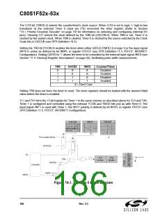
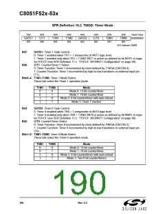
The C/T0 bit (TMOD.2) selects the counter/timer's clock source. When C/T0 is set to logic 1, high-to-low
transitions at the selected Timer 0 input pin (T0) increment the timer register (Refer to Section
“14.1. Priority Crossbar Decoder” on page 119 for information on selecting and configuring external I/O
pins). Clearing C/T selects the clock defined by the T0M bit (CKCON.3). When T0M is set, Timer 0 is
clocked by the system clock. When T0M is cleared, Timer 0 is clocked by the source selected by the Clock
Scale bits in CKCON (see SFR Definition 19.3).
Setting the TR0 bit (TCON.4) enables the timer when either GATE0 (TMOD.3) is logic 0 or the input signal
/INT0 is active as defined by bit IN0PL in register IT01CF (see SFR Definition 11.5. IT01CF: INT0/INT1
Configuration). Setting GATE0 to ‘1’ allows the timer to be controlled by the external input signal /INT0 (see
Section “11.4. Interrupt Register Descriptions” on page 93), facilitating pulse width measurements.
TR0
0
1
1
1
GATE0
/INT0
Counter/Timer
Disabled
X
0
1
1
X
X
0
1
Enabled
Disabled
Enabled
X = Don't Care
Setting TR0 does not force the timer to reset. The timer registers should be loaded with the desired initial
value before the timer is enabled.
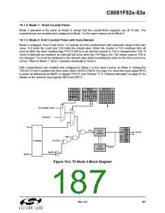
TL1 and TH1 form the 13-bit register for Timer 1 in the same manner as described above for TL0 and TH0.
Timer 1 is configured and controlled using the relevant TCON and TMOD bits just as with Timer 0. The
input signal /INT1 is used with Timer 1; the /INT1 polarity is defined by bit IN1PL in register IT01CF (see
SFR Definition 11.5. IT01CF: INT0/INT1 Configuration).
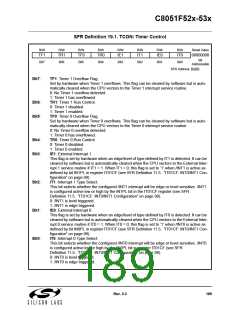
IT01CF
Figure 19.1. T0 Mode 0 Block Diagram
186
Rev. 0.3

 SILICON [ SILICON ]