C8051F52x-53x
The shift register contents are locked after the slave detects the first edge of SCK. Writes to SPI0DAT that
occur after the first SCK edge will be held in the TX latch until the end of the current transfer.
When configured as a slave, SPI0 can be configured for 4-wire or 3-wire operation. The default, 4-wire
slave mode, is active when NSSMD1 (SPI0CN.3) = 0 and NSSMD0 (SPI0CN.2) = 1. In 4-wire mode, the
NSS signal is routed to a port pin and configured as a digital input. SPI0 is enabled when NSS is logic 0,
and disabled when NSS is logic 1. The bit counter is reset on a falling edge of NSS. Note that the NSS sig-
nal must be driven low at least 2 system clocks before the first active edge of SCK for each byte transfer.
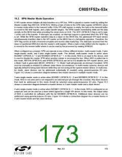
Figure 18.4 shows a connection diagram between two slave devices in 4-wire slave mode and a master
device.
3-wire slave mode is active when NSSMD1 (SPI0CN.3) = 0 and NSSMD0 (SPI0CN.2) = 0. NSS is not
used in this mode, and is not mapped to an external port pin through the crossbar. Since there is not a way
of uniquely addressing the device in 3-wire slave mode, SPI0 must be the only slave device present on the
bus. It is important to note that in 3-wire slave mode there is no external means of resetting the bit counter
that determines when a full byte has been received. The bit counter can only be reset by disabling and re-
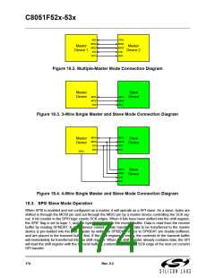
enabling SPI0 with the SPIEN bit. Figure 18.3 shows a connection diagram between a slave device in 3-
wire slave mode and a master device.
18.4. SPI0 Interrupt Sources
When SPI0 interrupts are enabled, the following four flags will generate an interrupt when they are set to
logic 1:
Note that all of the following interrupt bits must be cleared by software.
1. The SPI Interrupt Flag, SPIF (SPI0CN.7) is set to logic 1 at the end of each byte transfer. This
flag can occur in all SPI0 modes.
2. The Write Collision Flag, WCOL (SPI0CN.6) is set to logic 1 if a write to SPI0DAT is attempted
when the transmit buffer has not been emptied to the SPI shift register. When this occurs, the
write to SPI0DAT will be ignored, and the transmit buffer will not be written.This flag can occur
in all SPI0 modes.
3. The Mode Fault Flag MODF (SPI0CN.5) is set to logic 1 when SPI0 is configured as a master
in multi-master mode and the NSS pin is pulled low. When a Mode Fault occurs, the MSTEN
and SPIEN bits in SPI0CN are set to logic 0 to disable SPI0 and allow another master device
to access the bus.
4. The Receive Overrun Flag RXOVRN (SPI0CN.4) is set to logic 1 when configured as a slave,
and a transfer is completed while the receive buffer still holds an unread byte from a previous
transfer. The new byte is not transferred to the receive buffer, allowing the previously received
data byte to be read. The data byte which caused the overrun is lost.
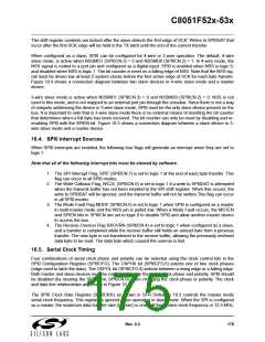
18.5. Serial Clock Timing
Four combinations of serial clock phase and polarity can be selected using the clock control bits in the
SPI0 Configuration Register (SPI0CFG). The CKPHA bit (SPI0CFG.5) selects one of two clock phases
(edge used to latch the data). The CKPOL bit (SPI0CFG.4) selects between a rising edge or a falling edge.
Both master and slave devices must be configured to use the same clock phase and polarity. SPI0 should
be disabled (by clearing the SPIEN bit, SPI0CN.0) when changing the clock phase or polarity. The clock
and data line relationships are shown in Figure 18.5.
The SPI0 Clock Rate Register (SPI0CKR) as shown in SFR Definition 18.3 controls the master mode
serial clock frequency. This register is ignored when operating in slave mode. When the SPI is configured
as a master, the maximum data transfer rate (bits/sec) is one-half the system clock frequency or 12.5 MHz,
Rev. 0.3
175

 SILICON [ SILICON ]