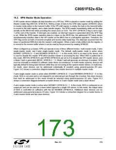
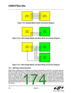
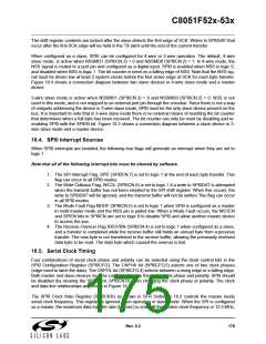
C8051F52x-53x
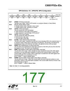
SFR Definition 18.1. SPI0CFG: SPI0 Configuration
R
R/W
R/W
CKPHA
Bit5
R/W
R
R
R
R
Reset Value
SPIBSY MSTEN
CKPOL SLVSEL
NSSIN
Bit2
SRMT
Bit1
RXBMT 00000111
Bit0
Bit7
Bit6
Bit4
Bit3
SFR Address: 0xA1
Bit 7:
SPIBSY: SPI Busy (read only).
This bit is set to logic 1 when a SPI transfer is in progress (Master or Slave Mode).
MSTEN: Master Mode Enable.
0: Disable master mode. Operate in slave mode.
1: Enable master mode. Operate as a master.
CKPHA: SPI0 Clock Phase.
Bit 6:
Bit 5:
This bit controls the SPI0 clock phase.
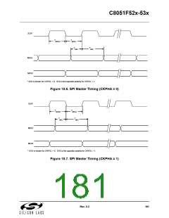
0: Data centered on first edge of SCK period.*
1: Data centered on second edge of SCK period.*
Bit 4:
Bit 3:
CKPOL: SPI0 Clock Polarity.
This bit controls the SPI0 clock polarity.
0: SCK line low in idle state.
1: SCK line high in idle state.
SLVSEL: Slave Selected Flag (read only).
This bit is set to logic 1 whenever the NSS pin is low indicating SPI0 is the selected slave. It
is cleared to logic 0 when NSS is high (slave not selected). This bit does not indicate the
instantaneous value at the NSS pin, but rather a de-glitched version of the pin input.
NSSIN: NSS Instantaneous Pin Input (read only).
This bit mimics the instantaneous value that is present on the NSS port pin at the time that
the register is read. This input is not de-glitched.
SRMT: Shift Register Empty (Valid in Slave Mode, read only).
This bit will be set to logic 1 when all data has been transferred in/out of the shift register,
and there is no new information available to read from the transmit buffer or write to the
receive buffer. It returns to logic 0 when a data byte is transferred to the shift register from
the transmit buffer or by a transition on SCK.
Bit 2:
Bit 1:
NOTE: SRMT = 1 when in Master Mode.
Bit 0:
RXBMT: Receive Buffer Empty (Valid in Slave Mode, read only).
This bit will be set to logic 1 when the receive buffer has been read and contains no new
information. If there is new information available in the receive buffer that has not been read,
this bit will return to logic 0.
NOTE: RXBMT = 1 when in Master Mode.
*Note: See Table 18.1 for timing parameters.
Rev. 0.3
177

 SILICON [ SILICON ]