C8051F52x-53x
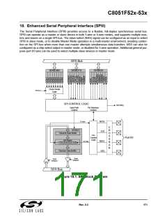
18.2. SPI0 Master Mode Operation
A SPI master device initiates all data transfers on a SPI bus. SPI0 is placed in master mode by setting the
Master Enable flag (MSTEN, SPI0CN.6). Writing a byte of data to the SPI0 data register (SPI0DAT) when
in master mode writes to the transmit buffer. If the SPI shift register is empty, the byte in the transmit buffer
is moved to the shift register, and a data transfer begins. The SPI0 master immediately shifts out the data
serially on the MOSI line while providing the serial clock on SCK. The SPIF (SPI0CN.7) flag is set to logic
1 at the end of the transfer. If interrupts are enabled, an interrupt request is generated when the SPIF flag
is set. While the SPI0 master transfers data to a slave on the MOSI line, the addressed SPI slave device
simultaneously transfers data to the SPI master on the MISO line in a full-duplex operation. Therefore, the
SPIF flag serves as both a transmit-complete and receive-data-ready flag. The data byte received from the
slave is transferred MSB-first into the master's shift register. When a byte is fully shifted into the register, it
is moved to the receive buffer where it can be read by the processor by reading SPI0DAT.
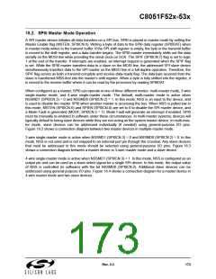
When configured as a master, SPI0 can operate in one of three different modes: multi-master mode, 3-wire
single-master mode, and 4-wire single-master mode. The default, multi-master mode is active when
NSSMD1 (SPI0CN.3) = 0 and NSSMD0 (SPI0CN.2) = 1. In this mode, NSS is an input to the device, and
is used to disable the master SPI0 when another master is accessing the bus. When NSS is pulled low in
this mode, MSTEN (SPI0CN.6) and SPIEN (SPI0CN.0) are set to 0 to disable the SPI master device, and
a Mode Fault is generated (MODF, SPI0CN.5 = 1). Mode Fault will generate an interrupt if enabled. SPI0
must be manually re-enabled in software under these circumstances. In multi-master systems, devices will
typically default to being slave devices while they are not acting as the system master device. In multi-mas-
ter mode, slave devices can be addressed individually (if needed) using general-purpose I/O pins.
Figure 18.2 shows a connection diagram between two master devices in multiple-master mode.
3-wire single-master mode is active when NSSMD1 (SPI0CN.3) = 0 and NSSMD0 (SPI0CN.2) = 0. In this
mode, NSS is not used and is not mapped to an external port pin through the crossbar. Any slave devices
that must be addressed in this mode should be selected using general-purpose I/O pins. Figure 18.3
shows a connection diagram between a master device in 3-wire master mode and a slave device.
4-wire single-master mode is active when NSSMD1 (SPI0CN.3) = 1. In this mode, NSS is configured as an
output pin and can be used as a slave-select signal for a single SPI device. In this mode, the output value
of NSS is controlled (in software) with the bit NSSMD0 (SPI0CN.2). Additional slave devices can be
addressed using general-purpose I/O pins. Figure 18.4 shows a connection diagram for a master device in
4-wire master mode and two slave devices.
Rev. 0.3
173

 SILICON [ SILICON ]