C8051F52x-53x
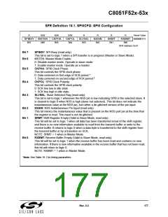
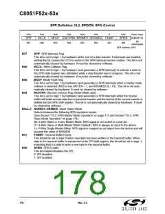
SFR Definition 18.2. SPI0CN: SPI0 Control
R/W
R/W
R/W
R/W
R/W
R/W
R
R/W
Reset Value
SPIF
WCOL
MODF RXOVRN NSSMD1 NSSMD0 TXBMT
SPIEN 00000110
Bit
Bit7
Bit6
Bit5
Bit4
Bit3
Bit2
Bit1
Bit0
Addressable
SFR Address: 0xF8
Bit7:
SPIF: SPI0 Interrupt Flag.
This bit is set to logic 1 by hardware at the end of a data transfer. If interrupts are enabled,
setting this bit causes the CPU to vector to the SPI0 interrupt service routine. This bit is not
automatically cleared by hardware. It must be cleared by software.
WCOL: Write Collision Flag.
This bit is set to logic 1 by hardware (and generates a SPI0 interrupt) to indicate a write to
the SPI0 data register was attempted while a data transfer was in progress. This bit is not
automatically cleared by hardware. It must be cleared by software.
MODF: Mode Fault Flag.
Bit6:
Bit5:
Bit4:
This bit is set to logic 1 by hardware (and generates a SPI0 interrupt) when a master mode
collision is detected (NSS is low, MSTEN = 1, and NSSMD[1:0] = 01). This bit is not auto-
matically cleared by hardware. It must be cleared by software.
RXOVRN: Receive Overrun Flag (Slave Mode only).
This bit is set to logic 1 by hardware (and generates a SPI0 interrupt) when the receive
buffer still holds unread data from a previous transfer and the last bit of the current transfer is
shifted into the SPI0 shift register. This bit is not automatically cleared by hardware. It must
be cleared by software.
Bits3–2: NSSMD1–NSSMD0: Slave Select Mode.
Selects between the following NSS operation modes:
(See Section “18.2. SPI0 Master Mode Operation” on page 173 and Section “18.3. SPI0
Slave Mode Operation” on page 174).
00: 3-Wire Slave or 3-wire Master Mode. NSS signal is not routed to a port pin.
01: 4-Wire Slave or Multi-Master Mode (Default). NSS is always an input to the device.
1x: 4-Wire Single-Master Mode. NSS signal is mapped as an output from the device and will
assume the value of NSSMD0.
Bit1:
Bit0:
TXBMT: Transmit Buffer Empty.
This bit will be set to logic 0 when new data has been written to the transmit buffer. When
data in the transmit buffer is transferred to the SPI shift register, this bit will be set to logic 1,
indicating that it is safe to write a new byte to the transmit buffer.
SPIEN: SPI0 Enable.
This bit enables/disables the SPI.
0: SPI disabled.
1: SPI enabled.
178
Rev. 0.3

 SILICON [ SILICON ]