C8051F52x-53x
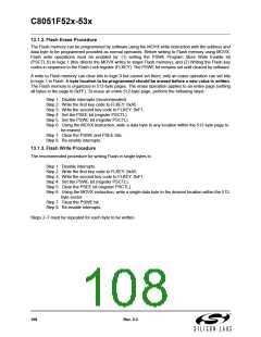
For block Flash writes, the Flash write procedure is only performed after the last byte of each block is writ-
ten with the MOVX write instruction. A Flash write block is two bytes long, from even addresses to odd
addresses. Writes must be performed sequentially (i.e. addresses ending in 0b and 1b must be written in
order). The Flash write will be performed following the MOVX write that targets the address ending in 1b. If
a byte in the block does not need to be updated in Flash, it should be written to 0xFF. The recommended
procedure for writing Flash in blocks is:
Step 1. Disable interrupts.
Step 2. Write the first key code to FLKEY: 0xA5.
Step 3. Write the second key code to FLKEY: 0xF1.
Step 4. Set the PSWE bit (register PSCTL).
Step 5. Clear the PSEE bit (register PSCTL).
Step 6. Using the MOVX instruction, write the first data byte to the even block location (ending in
0b).
Step 7. Clear the PSWE bit (register PSCTL).
Step 8. Write the first key code to FLKEY: 0xA5.
Step 9. Write the second key code to FLKEY: 0xF1.
Step 10. Set the PSWE bit (register PSCTL).
Step 11. Clear the PSEE bit (register PSCTL).
Step 12. Using the MOVX instruction, write the second data byte to the odd block location (ending
in 1b).
Step 13. Clear the PSWE bit (register PSCTL).
Step 14. Re-enable interrupts.
Steps 2–13 must be repeated for each block to be written.
13.2. Flash Write and Erase Guidelines
Any system which contains routines which write or erase Flash memory from software involves some risk
that the write or erase routines will execute unintentionally if the CPU is operating outside its specified
operating range of V , system clock frequency, or temperature. This accidental execution of Flash modi-
DD
fying code can result in alteration of Flash memory contents causing a system failure that is only recover-
able by re-Flashing the code in the device.
The following guidelines are recommended for any system which contains routines which write or erase
Flash from code.
Rev. 0.3
109

 SILICON [ SILICON ]