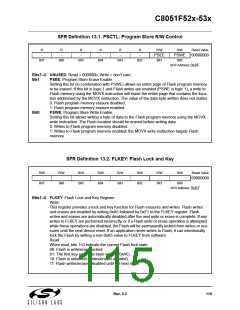
C8051F52x-53x
13.2.2. PSWE Maintenance
7. Reduce the number of places in code where the PSWE bit (b0 in PSCTL) is set to a '1'. There
should be exactly one routine in code that sets PSWE to a '1' to write Flash bytes and one rou-
tine in code that sets PSWE and PSEE both to a '1' to erase Flash pages.
8. Minimize the number of variable accesses while PSWE is set to a '1'. Handle pointer address
updates and loop variable maintenance outside the "PSWE = 1; ... PSWE = 0;" area. Code
examples showing this can be found in AN201, "Writing to Flash from Firmware", available
from the Silicon Laboratories web site.
9. Disable interrupts prior to setting PSWE to a '1' and leave them disabled until after PSWE has
been reset to '0'. Any interrupts posted during the Flash write or erase operation will be ser-
viced in priority order after the Flash operation has been completed and interrupts have been
re-enabled by software.
10. Make certain that the Flash write and erase pointer variables are not located in XRAM. See
your compiler documentation for instructions regarding how to explicitly locate variables in dif-
ferent memory areas.
11. Add address bounds checking to the routines that write or erase Flash memory to ensure that
a routine called with an illegal address does not result in modification of the Flash.
13.2.3. System Clock
12. If operating from an external crystal, be advised that crystal performance is susceptible to
electrical interference and is sensitive to layout and to changes in temperature. If the system is
operating in an electrically noisy environment, use the internal oscillator or use an external
CMOS clock.
13. If operating from the external oscillator, switch to the internal oscillator during Flash write or
erase operations. The external oscillator can continue to run, and the CPU can switch back to
the external oscillator after the Flash operation has completed.
Additional Flash recommendations and example code can be found in AN201, "Writing to Flash from Firm-
ware", available from the Silicon Laboratories web site.
Rev. 0.3
111

 SILICON [ SILICON ]