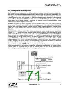
C8051F39x/37x
The Comparator response time may be configured in software via the CPT0MD register (see SFR Defini-
tion 14.2). Selecting a longer response time reduces the Comparator supply current.
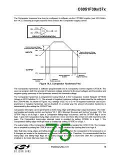
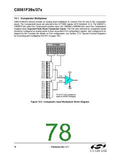
CP0+
VIN+
VIN-
+
CP0
_
OUT
CP0-
CIRCUIT CONFIGURATION
Positive Hysteresis Voltage
(Programmed with CP0HYP Bits)
VIN-
Negative Hysteresis Voltage
INPUTS
(Programmed by CP0HYN Bits)
VIN+
VOH
OUTPUT
VOL
Negative Hysteresis
Disabled
Maximum
Negative Hysteresis
Positive Hysteresis
Disabled
Maximum
Positive Hysteresis
Figure 14.2. Comparator Hysteresis Plot
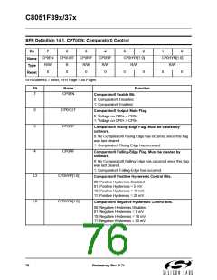
The Comparator hysteresis is software-programmable via its Comparator Control register CPT0CN. The
user can program both the amount of hysteresis voltage (referred to the input voltage) and the positive and
negative-going symmetry of this hysteresis around the threshold voltage.
The Comparator hysteresis is programmed using Bits3–0 in the Comparator Control Register CPT0CN
(shown in SFR Definition 14.1). The amount of negative hysteresis voltage is determined by the settings of
the CP0HYN bits. As shown in Figure 14.2, settings of 20, 10, or 5 mV of negative hysteresis can be pro-
grammed, or negative hysteresis can be disabled. In a similar way, the amount of positive hysteresis is
determined by the setting the CP0HYP bits.
Comparator interrupts can be generated on both rising-edge and falling-edge output transitions. (For Inter-
rupt enable and priority control, see Section “20.1. MCU Interrupt Sources and Vectors” on page 116). The
CP0FIF flag is set to logic 1 upon a Comparator falling-edge occurrence, and the CP0RIF flag is set to
logic 1 upon the Comparator rising-edge occurrence. Once set, these bits remain set until cleared by soft-
ware. The Comparator rising-edge interrupt mask is enabled by setting CP0RIE to a logic 1. The
Comparator0 falling-edge interrupt mask is enabled by setting CP0FIE to a logic 1.
The output state of the Comparator can be obtained at any time by reading the CP0OUT bit. The Compar-
ator is enabled by setting the CP0EN bit to logic 1, and is disabled by clearing this bit to logic 0.
Note that false rising edges and falling edges can be detected when the comparator is first powered on or
if changes are made to the hysteresis or response time control bits. Therefore, it is recommended that the
rising-edge and falling-edge flags be explicitly cleared to logic 0 a short time after the comparator is
enabled or its mode bits have been changed.
Preliminary Rev. 0.71
75

 SILICON [ SILICON ]